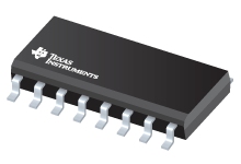
Datasheet Texas Instruments SN65LVDS104PW
| Manufacturer | Texas Instruments |
| Series | SN65LVDS104 |
| Part Number | SN65LVDS104PW |

1:4 LVDS Clock Fanout Buffer 16-TSSOP -40 to 85
Datasheets
SN65LVDS10x 4-Port LVDS and 4-Port TTL-to-LVDS Repeaters datasheet
PDF, 1.2 Mb, Revision: G, File published: Dec 31, 2015
Extract from the document
Status
| Lifecycle Status | Active (Recommended for new designs) |
| Manufacture's Sample Availability | Yes |
Packaging
| Pin | 16 |
| Package Type | PW |
| Industry STD Term | TSSOP |
| JEDEC Code | R-PDSO-G |
| Package QTY | 90 |
| Carrier | TUBE |
| Device Marking | LVDS104 |
| Width (mm) | 4.4 |
| Length (mm) | 5 |
| Thickness (mm) | 1 |
| Pitch (mm) | .65 |
| Max Height (mm) | 1.2 |
| Mechanical Data | Download |
Parametrics
| Input Frequency(Max) | 400 MHz |
| Input Level | LVDS |
| Number of Outputs | 4 |
| Operating Temperature Range | -40 to 85 C |
| Output Frequency(Max) | 400 MHz |
| Output Level | LVDS |
| Package Group | TSSOP |
| Package Size: mm2:W x L | 16TSSOP: 32 mm2: 6.4 x 5(TSSOP) PKG |
| Rating | Catalog |
| VCC | 3.3 V |
| VCC Out | 3.3 V |
Eco Plan
| RoHS | Compliant |
Application Notes
- DC-Coupling Between Differential LVPECL, LVDS, HSTL, and CMLPDF, 135 Kb, File published: Feb 19, 2003
- AC Coupling Between Differential LVPECL, LVDS, HSTL and CML (Rev. C)PDF, 417 Kb, Revision: C, File published: Oct 17, 2007
This report provides a quick reference of ac-coupling techniques for interfacing between different logic levels. The four differential signaling levels found in this reportare low-voltage positive-referenced emitter coupled logic (LVPECL), low-voltage differential signals (LVDS), high-speed transceiver logic (HSTL), and current-modelogic (CML). From these four differential signaling levels, 16
Model Line
Series: SN65LVDS104 (8)
Manufacturer's Classification
- Semiconductors > Clock and Timing > Clock Buffers > Differential