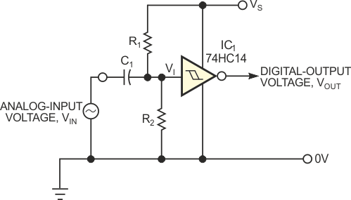
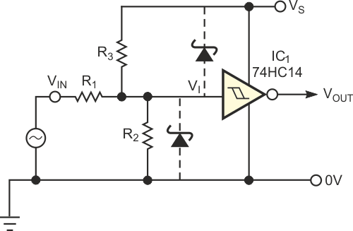
The circuit in Figure 1 shows a familiar technique for converting a low-level analog signal to digital form. Resistors R1 and R2 set the quiescent dc level at the Schmitt inverter's input to a value roughly equal to the midpoint of the hysteresis band. Capacitor C1 removes dc content from VIN, such that the Schmitt trigger's input signal, VI, centers itself on the midhysteresis level. Provided that VIN is large enough to cross IC1’s threshold level, the output signal, VOUT, provides a faithful digital representation of VIN. Unfortunately, the circuit suffers from several drawbacks. The presence of C1 makes it impossible for IC1 to switch at specifically defined dc levels on VIN. Furthermore, for low-frequency waveforms, C1 must be extremely large to prevent unwanted signal attenuation. Also, if VIN is of random period or is asymmetrical with time (for example, a pulse train with low duty cycle), the signal at VI will not swing symmetrically about the quiescent dc level and may fail to cross one of IC1’s thresholds. You can solve all these problems by replacing C1 with a resistor, as in Figure 2.
 |
|
| Figure 1. | This Schmitt-trigger circuit is useful for converting an ac signal to digital form. |
 |
|
| Figure 2. | Eliminating the input capacitor avoids problems with asymmetrical input waveforms. |
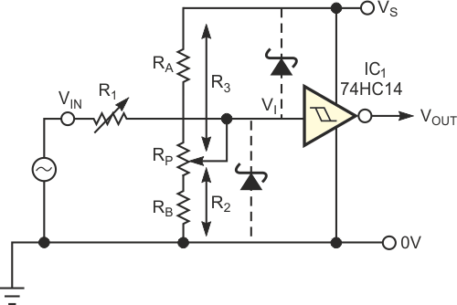
In Figure 2, R1 and the parallel combination of R2 and R3 act as an attenuator that allows IC1 to switch at specific, user-defined dc levels that may be much greater than IC1’s switching thresholds. Furthermore, R2 and R3 introduce an offset that allows VIN’s lower threshold to be negative if required. R1 and R2 relate to R3 as follows:
where VS is the supply voltage; VP and VN are the required upper and lower VIN thresholds, respectively; and VTU and VTL are the Schmitt trigger's upper and lower switching thresholds. By measuring VTU and VTL for a given Schmitt inverter and selecting a suitable value for R3, you can calculate the corresponding values of R1 and R2. The circuit accommodates almost any values of VP and VN. The only restriction is that the hysteresis (VP – VN) is sufficiently larger than IC1’s hysteresis (VTU – VTL); otherwise, the equations can yield negative resistor values. If IC1 is a CMOS device (for example, 74HC14, 74AC14, 4093B, or 40106B), you can use large resistances, thus ensuring high input impedance.
 |
|
| Figure 3. | The potentiometer networks solve the problem of large spreads in component values. |
For cases in which it is inconvenient to measure the exact values of VTU and VTL, you can replace R1 and R2 with variable resistors to accommodate the worst-case spread in VTU and VTL. However, because R2 and R3 have a large influence on R1, the spread of values you need for R2 results in a broad variation in the R2-R3 parallel combination and results in an even broader spread of values for R1. Replacing R2 and R3 with a potentiometer network, as in Figure 3, provides a solution to the “spread” problem. Because R2 varies with R3, the spread in the R2-R3 parallel combination, and hence in R1, is narrower. This arrangement results in some fairly onerous equations relating the variables. However, you can simplify matters by observing that for a particular CMOS Schmitt inverter, each of its thresholds is a constant fraction of the supply voltage, VS. Therefore, you can define VTU = UVS and VTL = LVS, where U and L are the respective fractions. This simplification results in the following equations:
and
The design procedure is to select the desired values for VS, VP, and VN and then to calculate R1, R2, and R3 in terms of RX for the worst-case spread in U and L. You can then scale the values of R1, R2, and R3 accordingly. As an example, assume that you need to set VP at 6 V and VN at –7.5 V using a 74HC14 operating from a 5 V supply. Although slight differences exist between manufacturers, the “typical” spread in thresholds for the 74HC14 on a 5 V rail yields the following values: U = 0.5 (minimum) to 0.7 (maximum), and L = 0.2 (minimum) to 0.44 (maximum). These values are subject to the restrictions on hysteresis: (U-L) = 0.09 (minimum) to 0.5 (maximum). You can intuitively see that R1 is at a maximum when IC1’s hysteresis is small and the parallel combination of R2 and R3 is large. This scenario occurs when IC1 has a narrow hysteresis band centered roughly on VS/2. In this example, R1 is a maximum of 7.25RX when L = 0.435 and U = 0.525. Conversely, R1 is at a minimum when IC1’s hysteresis is large and the parallel combination of R2 and R3 is small. This scenario occurs when L = 0.2 and U = 0.7, resulting in R1 = 1.067RX. The range of potentiometer RP must allow you to set the quiescent value of VI anywhere from the minimum midhysteresis band level (occurring when L and U are both minima), to the maximum midhysteresis level (occurring when L and U are both maxima). In this example, the values are R2 = 0.4125RX and R3 = 0.5875RX (when L = 0.2 and U = 0.5) and R2 = 0.6467RX and R3 = 0.3533RX (when L = 0.44 and U = 0.7). Assuming that you use resistors with ±1% tolerance and potentiometers with ±10% tolerance, you can accommodate the required spread in R2 and R3 with an adequate margin by making RA = 1.1 kΩ, RP = 1 kΩ, and RB = 1.3 kΩ. The corresponding spread in R1 (including the tolerance in RX itself) is 3.495 to 25.549 kΩ. You can obtain this range by using a parallel connection of a 50-kΩ potentiometer and a 51-kΩ resistor that is in series with a 3.3-kΩ resistor.
 |
|
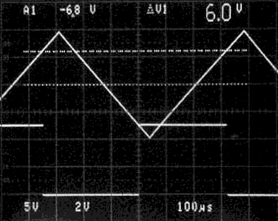
| Figure 4. | These waveforms indicate clean hysteretic switching with a triangle- wave input.ometer networks solve the problem of large spreads in component values. |
The oscilloscope screen in Figure 4 illustrates the performance of the example circuit, in which VIN is a ±10 V triangle wave. By adjusting the two potentiometers in turn, we made the output waveform switch when VIN = 6 V and –7.5 V. Despite the interaction between the potentiometers, you can fairly easily (with a little patience) set the thresholds. Although the circuit is not intended for precision applications, it does extend the range of the garden-variety Schmitt inverter and allows you to implement positive and negative thresholds of several tens or even hundreds of volts. Moreover, the circuit allows VN to be positive, provided that VP is sufficiently greater than VN to avoid negative resistance values. You can obtain operation of greater than 10-MHz frequency if you use suitable devices for IC1. The 74AC14 or 74HC14 yield response times of just a few nanoseconds with a rail-to-rail output. For best high-frequency performance, use low resistor values, a shunt trimmer capacitor across R1 to provide compensation, or both. Finally, use Schottky clamp diodes as in Figure 3 to protect the inputs of IC1 from overvoltage conditions.
