One of the first problems a capacitive-sensor analog designer must face is the low-frequency cutoff. Theoretically, you must fulfill just one simple requirement: a sufficiently large input resistance of the preamplifier's first stage. In practice, however, many problems lurk behind the seemingly straightforward design rules. First, the preamplifier's active device must have a defined dc operating point. Using field-effect devices renders the dc input current of the first active device (a JFET or a MOSFET) so low that you can neglect it in most cases. On the other hand, the circuit must have some dc-path-creating resistor to present the required dc potential to the input electrode. Assuming that a typical miniature capacitive sensor, such as a high-quality capacitive microphone, has a small capacitance of 20 to 50 pF, for example, the resistor value to obtain a cutoff frequency as high as 50 Hz would be on the order of 108 to 109 Ω. Resistors with such high values are difficult to find in SMD formats, are expensive, have poor accuracy and stability, and are large and noisy. Moreover, further difficulties appear when the capacitive sensor requires an external polarization voltage. Such a polarization voltage may have a value of 100 V or more. This voltage must connect to the sensor via a separate circuit, and it sometimes creates problems if the need to have at least one side of the sensor grounded emerges. And, as in all similar cases, the preamplifier should be as close to the sensor as possible. It should consume minimal space, need few connecting leads, and produce as little heat as possible. The circuit in Figure 1 represents one possible approach to meeting these challenges.
 |
|
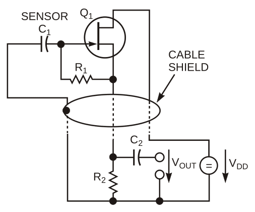
| Figure 1. | The JFET in this circuit effectively multiplies the value of R1. |
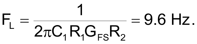
The circuit uses electronic multiplication of the gate resistor, R1, value via positive feedback through the source-follower action of JFET Q1. The multiplication factor is α = GFSR2. (Note: GFS is the real part of the differential forward transfer admittance in common-source connection.) Assuming a typical value of C1 = 33 pF, reasonable values of R1 = 10 MΩ and R2 = 10 kΩ and assuming a conservative value of GFS = 5 mA/V (typical in the JFET type BF245B at VGS = 0 V and VDS = 15 V), you obtain the following low-frequency cutoff:
With this method, notwithstanding the extremely small sensor capacitance and conservative values of all other components, you obtain a respectable cutoff frequency. At the same time, to get the required high polarizing voltage VPOL to the sensor while keeping one side connected directly to ground, you can use a supply voltage, VDD = VDS + VPOL = 115 V, where VPOL = IDR2, and ID is the JFET's drain current at the selected VDS and VGS = 0. Thus, you provide a polarizing voltage of 100 V to the sensor. Other advantages of the circuit are obvious at the first glance: Only two elements of the circuit, R1 and Q1, must be connected directly at the sensor's location. Both these components are readily available, and they are physically small (usually considerably smaller than the sensor itself), so they pose no space problems. The heat the JFET produces – 150 mW – is low enough to be negligible in most applications. The circuit needs only three wires for connection, and one of them can also serve as cable shielding. The connecting cable can be quite long; its maximum length is limited primarily by its capacitance, which determines the upper cutoff frequency. In most applications, the upper cutoff frequency of the sensor itself is low enough to permit a rather long cable. The only minor disadvantage of the circuit lies in its total power consumption, mostly dissipated in R2 (1 W in this case).
 |
|
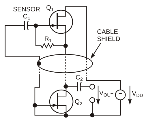
| Figure 2. | The second JFET, Q2, in this circuit replaces R2 in the circuit of Figure 1. |
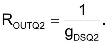
In cases not requiring a high polarizing voltage, the value of R2 might become too small to obtain a sufficiently large multiplication factor, α. Then, another JFET, Q2, can replace R2 (Figure 2). This JFET has its gate shorted to its source and operates as a constant-current source. You can calculate the R1 multiplication factor α from the same formula as for Figure 1, with the R2 value replaced by the value of
You must lower the overall supply voltage, VDD, accordingly to provide the same operating point for Q1. The processing stage, the amplifying stage, or both immediately following the preamplifier should not have too small a differential input resistance; this resistance appears in parallel with R2 or Q2, so it reduces the multiplication factor, α. A noninverting input of an operational amplifier easily satisfies this requirement.
Choosing a less common but still reasonable value of R1 = 100 MΩ pushes the low-frequency cutoff below 1 Hz with no other changes in the circuit necessary. The dynamic range of the preamplifier is respectable. The maximum permissible positive swing of the input voltage is equal to the forward threshold voltage of Q1’s gate-insulating p-n junction multiplied by the same multiplication factor, α, as the input resistance. In the circuit of Figure 1, with the cited component values, at a 300 K temperature and VDD = 115 V, the permissible swing exceeds 5 V peak. The JFET alone determines the noise figure; hence, it is rather low. The maximum permissible negative swing of the input voltage is usually much larger. A second possible solution of the low-frequency-cutoff problem in capacitive-sensor analog preamplifiers appears in the case of electret-biased sensors. These sensors need no external polarizing voltage, thus simplifying the overall power-supply design. In these cases, you can achieve an even larger multiplication factor of the biasing resistance by applying unity positive voltage feedback in an operational amplifier (Figure 3).
 |
|
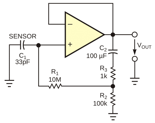
| Figure 3. | An operational amplifier provides yet another means to achieve high impedance for capacitive sensors. |
To obtain a full unity positive voltage feedback in the circuit, the value of R3 should be zero. A minor complication exists, however. To prevent dc instability (bistable flip-flop behavior), a dc path in the positive-feedback circuit must not exist. C2 is the dc-blocking device. Unfortunately, C2 introduces another pole in the transfer function of the circuit. To render its effects negligible, C2 would need an uncomfortably large value. As long as you are prepared to sacrifice a bit of the otherwise extremely large R1 -value multiplication factor, α (theoretically equal to the open-loop voltage gain of the operational amplifier, or 105, typically), you can use a C2 value several orders of magnitude smaller under the condition that doing so introduces some additional damping into the circuit by means of a nonzero value of R3. R2 is necessary to provide a correct dc potential (quiescent operating-point conditions) for the noninverting input of the operational amplifier.
A detailed analysis of the circuit in terms of stability and its response to harmonic and step-signal drive is rather lengthy. You can base the analysis on the rules of general active-filter theory, or you can simulate the circuit behavior with any of the common simulation tools, such as Spice. By an intelligent choice of passive-component values, you can easily control the circuit's behavior in terms of low-frequency cutoff. Thus, you can obtain a maximally flat frequency response or a maximally flat transient response or set a predetermined amount of overshoot in the response to a step input, for example. The operational amplifier must have quiescent dc currents of both inputs as low as possible. CMOS op amps are best in this respect. The circuit of Figure 3 requires a somewhat larger space for components in the immediate vicinity of the sensor, as well as four instead of three connecting leads. On the other hand, it is less sensitive to external loads than are the circuits in Figure 1 or Figure 2.
The op amp in Figure 3 is a TS271, a CMOS op amp from STMicroelectronics. The low-frequency cutoff is at 7 Hz, and the step-response overshoot is 0%. With larger values of C2 and smaller values of R3, you can easily achieve a low-frequency cutoff of 0.1 Hz or lower. The circuit in Figure 3 is well-suited for micropower applications. Using a micropower CMOS operational amplifier, you can reliably obtain 10 years of unattended operation with standard passive components and just a single coin-sized lithium cell as the power source. The properties of the operational amplifier fully determine the high frequency cutoff and dynamic range of the circuit in Figure 3.
