The simple current-limiting load switch shown in Figure 1 will be familiar to most readers. In this circuit, a high level signal applied to the input switches on MOSFET Q2, which energizes the load. The load current is limited by negative feedback applied via Q1.
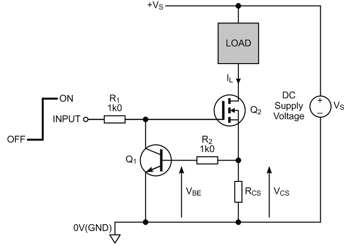 |
|
| Figure 1. | Simple, linear current limiter. |
In most applications, the current flowing via R2 into Q1's base will be very small compared to the load current IL, so the voltage VCS developed across current-sensing resistor RCS is roughly equal to Q1's base-emitter voltage, VBE. Therefore,
VBE ≈ VCS,
and since
VCS = ILRCS,
it follows that
VBE ≈ ILRCS,
or

The value of RCS is chosen to limit the load current to a maximum value determined by

where VBE(ON) is the base-emitter voltage needed to bias Q1 into conduction. At room temperature, VBE(ON) ≈ 650 mV. So, for example, a value of RCS = 3.3 Ω would set IL(MAX) to around 200 mA.
Under normal, 'no-fault' conditions, where IL is within normal limits, VBE is too small to bias Q1 on, such that MOSFET Q2 remains fully enhanced by the high level signal applied to its gate via R1. Under these conditions, the load current is determined mainly by the load resistance and the supply voltage, VS. However, if a fault causes IL to approach IL(MAX), Q1 starts to conduct, and reduces Q2’s gate-source voltage to a level that holds the load current roughly constant, at a value given by:
This linear current limiter is very effective for applications where IL(MAX) and the supply voltage are not too large. However, the circuit’s ability to limit the load current safely is determined by the power dissipated in Q2. For example, if RCS is selected to set IL(MAX) to 400 mA and if VS = 12 V, a short circuit across the load would dissipate almost 5 W in Q2. Not only must Q2 be capable of handling this power with adequate margin, but additional heat-sinking may be required to keep its junction temperature at a safe level. Larger values of IL(MAX) and/or VS would simply exacerbate this problem.
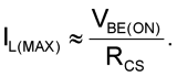
However, by adding just two inexpensive components, you can adapt the circuit to provide effective current limiting with none of the power dissipation problems. The resulting Design Idea in Figure 2 functions as a latching circuit breaker.
 |
|
| Figure 2. | Load switch with circuit breaker protection. |
To understand how the circuit works, assume that INPUT is high, Q2 is on, and normal current is flowing in the load. Under these conditions, the voltage across RCS is less than VBE(ON), and so Q1 has insufficient bias to conduct fully. Any slight leakage current in Q1's collector is diverted away from Q3's base via R3 which clamps the PNP's base-emitter junction voltage to a few millivolts or less, thereby holding Q3 off. Provided the load current remains within normal limits, both Q1 and Q3 remain off and have no effect on Q2.
As with the simple current-limiter of Figure 1, a load fault resulting in excessive load current will increase the voltage across RCS above the 650 mV needed to turn on Q1. However, additional transistor Q3 acts with Q1 to form an SCR-like structure; when Q1 turns on, it floods Q3's base with current, which itself turns on hard, sourcing more current into Q1's base. This positive feedback around Q1 and Q3 ensures that they both rapidly turn on hard.
R2 is necessary to ensure that most of Q3's collector current flows into Q1's base, effectively isolating Q3's collector from the relatively low resistance of RCS. With Q1 and Q3 both switched on hard, Q2's gate voltage relative to 0 V is clamped to a low value, typically around 800 mV or so. Since most N-channel MOSFET's need a gate-source voltage of at least 2 V to switch on, Q2 now turns off rapidly and the load current and the voltage across RCS fall to zero. However, since Q1 and Q3 are both latched on, the MOSFET remains off, thereby protecting it from overheating.
The circuit breaker can be reset simply by taking the INPUT signal to 0 V, which deprives Q1 and Q3 of current such that they both turn off. Taking the INPUT high again will switch on Q2, and normal operation will resume only if the load fault has been removed. If the load fault persists, the circuit breaker will immediately 'trip' and switch off the MOSFET.
The resistor values shown in the figure should be adequate for most applications. Make sure that the value of R1 is not too small, otherwise excessive current could flow into the INPUT terminal whenever Q1 and Q3 are latched on. The MOSFET should be selected mainly to handle the maximum load current and supply voltage requirements. Most general-purpose transistors with good current gain are suitable for Q1 and Q3.
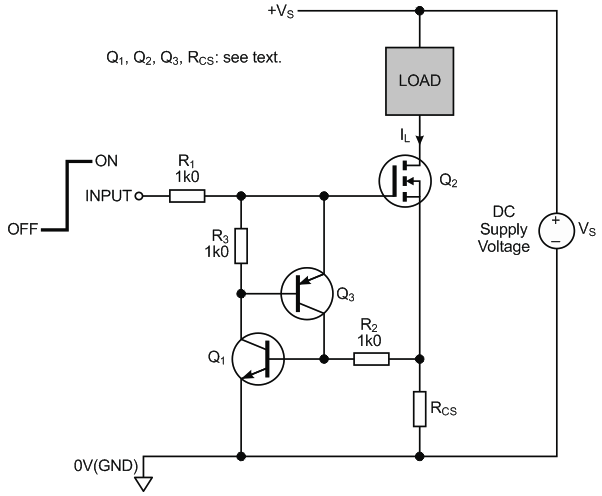
 |
|
| Figure 3. | Oscillograph illustrating circuit behavior: Top: INPUT (5 V/div); Middle: Q2 Drain (1 V/div); Bottom: Voltage across RCS (500 mV/div). |
The oscillograph in Figure 3 illustrates the performance of the circuit. Here, RCS was chosen for a trip point of IL(MAX) = 150 mA and the 20 Ω load was powered from a supply voltage VS = 5 V. The top trace shows the INPUT signal switching from 0 V to 5 V, the middle trace is the voltage at Q2's drain, and the bottom trace shows the voltage across RCS. When the INPUT signal goes high, Q2 initially turns on and its drain voltage begins its transition from 5 V toward 0 V as current flows through the load. However, since the 20 Ω load resistance results in a load current exceeding 150 mA, the voltage across RCS quickly rises above 650 mV, causing the circuit breaker to trip.
The circuit works well with loads such as relays, LEDs, and so on. However, as can be seen from Figure 3, the circuit breaker is very fast, taking less than 150 ns to respond to the overload and latch into the 'off' state. Therefore, loads such as motors, filament bulbs, and capacitive loads, which exhibit a relatively large 'inrush' current, may cause false tripping.