Pulse generators often need voltage comparators with accurately defined hysteresis, and such comparators need bipolar voltage references. Most voltage-reference-cell ICs are referenced to their low-side supply rail. If your circuit needs both positive and negative voltages, you could create the negative reference voltage by connecting a –1 gain inverter to the output of an IC reference cell. If your analog circuit runs from a single power supply, however, you must shift the common-mode voltage to a specific level. You can use the circuit in Figure 1 for that task.
 |
||
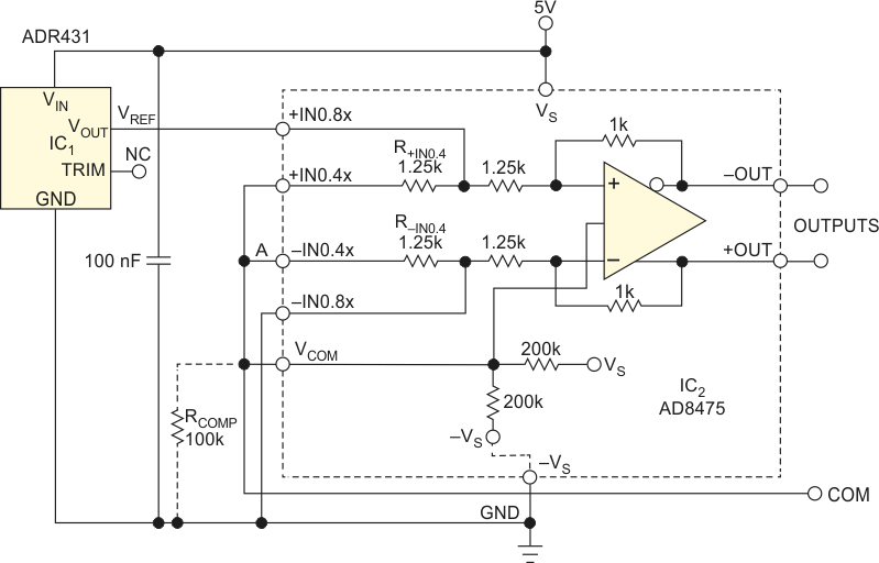
| Figure 1. | You can use this circuit to generate precision reference voltages of 1, –1, 1.25, and –1.25 V. | |
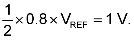
Reference cell IC1’s output voltage, VREF, connects to the noninverting input of amplifier IC2, an AD8475. This high-precision, differential-output, ×0.4/×0.8 amplifier in this case connects as an ×0.8 amplifier. The negative input, –IN, of IC2 is grounded. Voltages at its positive and negative outputs form the positive- and negative-output reference voltage, referenced to common-mode voltage VCOM. The magnitude of the generated reference voltages is
The AD8475’s gains of 0.4 and 0.8 have a tolerance of no more than 0.05% because of the device’s laser-trimmed internal gain-setting resistors. This circuit takes advantage of the AD8475’s gain-setting options. Typical use of the device as a ×0.8 amplifier keeps the +VIN0.4× and –VIN0.4× unconnected. In the circuit in Figure 1, however, these inputs interconnect, forming a high-precision 1-to-1 voltage divider of VREF.
The VCOM input of the AD8475 connects to this node, and the common-mode voltage of the generated reference voltages becomes VREF/2. Case A in Table 1 shows that the measured common-mode voltage is approximately 0.6% lower than VREF/2. This difference stems from the fact that the VCOM input connects within the AD8475 through one 200-kΩ resistor to the VS pin and through another 200-kΩ resistor to ground. You can, therefore, model the VCOM input as a source of VS/2 = 2.5 V with a series resistance of 100 kΩ. This series resistance acts as if it connects in parallel to the R+VIN0.4× resistor, which results in a slight imbalance in the 1-to-1 divider ratio. In cases B and C, the VCOM pin connects to Point A. The compensation resistor connects only in Case C. You can prove from the VGND values in cases B and C that RCOMP pushes the relative error of voltage at the COM output from 0.632% to –0.032%.
| Table 1. | Output voltages and voltage at VCOM pin | ||||||||||||||||||||
|
|||||||||||||||||||||
In many applications, the magnitude of difference of bipolar reference voltages is important, and this imbalance has no effect on it. If, however, your application requires a high-accuracy common-mode voltage, you can connect a 100-kΩ compensation resistor between the VCOM pin and ground, and the circuit thus operates as in Case C. This approach almost fully retains the accuracy of the 1-to-1 divider ratio.