Ilija Uzelac
Electronic Design
This circuit uses a few standard discrete components to provide a user-settable current-limit function with closed-loop performance. In addition, the limiter function can be turned on and off via an external digital control line, such as from a microcontroller output pin, via an optocoupler that is part of the circuit.
A current-limiting circuit is often needed to protect the most expensive parts of the circuit from transients such as current spikes, which occur when a power supply is driving a large capacitive load, an H-bridge is starting an inductive motor, or a current-limiter circuit is driving power LEDs.
 |
||
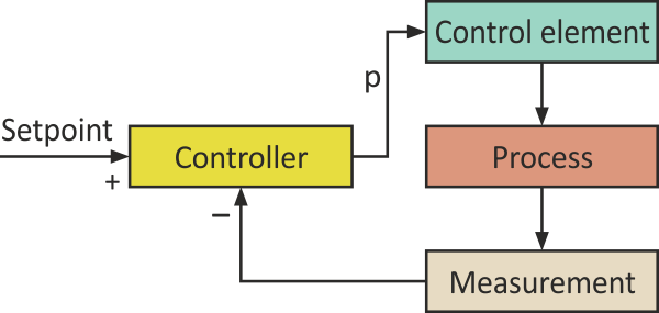
| Figure 1. | The design begins with a standard closed-loop control approach, comparing the desired setpoint value of the maximum allowed current to the actual value, and a control signal p. |
|
This versatile high-side current limiter uses negative-feedback control based on general process-control principles (Fig. 1). Figure 2 illustrates a practical implementation. Here, the process being controlled is the output current, which has very nearly the same value as the input current. A measurement is performed across the sense resistor R1. Its value defines the setpoint (the maximum allowed current).
 |
||
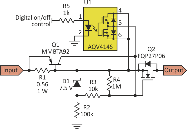
| Figure 2. | The closed-loop function includes Q1’s collector current as the control signal and R3/Q2 as the loop-control element, with the loop’s setpoint established by the current through R1. |
|
PNP transistor Q1 represents the controller, while its collector current ICQ1 is the control signal p. Resistor R3 and the P-channel MOSFET Q2 together form the control element. It is important to emphasize that the controller doesn’t perform any action on the control element (the control signal p is zero) until the input current reaches the setpoint current.
Transistor Q2 is not conducting at power-on until the input voltage reaches the VGS threshold voltage, which for most MOSFETs is 3 to 5 V, and the further increase of the input voltage fully turns on Q2. Therefore, Q2 can act as a switch, assuming that the input current hasn’t yet reached the setpoint current. The VGS voltage is limited by the choice of the Zener diode D1, which is 7.5 V in this particular design.
The PNP transistor chosen (MMBTA92) has a VBE threshold voltage of approximately 0.56 V. With R1 equal to 0.56 Ω, this sets the current limit to 1 A. Q1 starts to conduct when the voltage across R1 exceeds 0.56 V or when the input current exceeds 1 A. Its collector current then starts to flow through
Based on the relationship that
VGS = 7.5 – R3 × ICQ1,
any increase in the collector current of Q1 (the control signal p) decreases voltage VGS and subsequently decreases the output current of Q2, which in turn decreases the voltage across R1. This completes the negative feedback loop. It is important to note that in the control mode (ICQ1 > 0), Q2 operates in an active mode. So, it is necessary to observe the safe operating area (SOA) of a chosen MOSFET.
The voltage of Zener diode D1 needs to be larger than the required VGS voltage, corresponding to the maximum (limited) output current. R3 determines the sensitivity of the control element. While higher values will make the control loop more responsive, this will also increase the loop gain, which may lead to oscillations around the setpoint. A value of R3 = 10 kΩ was determined empirically as the optimal value without oscillations in the output current around the setpoint.
The addition of a small solid-state relay driven directly from a microcontroller pin allows external ON/OFF control of the limiting function. Optocoupler-MOSFET U1 (AQV414) is a normally closed device that holds Q2 switched off when the digital control input is low and allows Q2 to be conductive when it is high. Resistor R4 ensures that the gate-source capacitance of Q2 is completely discharged when the circuit is powered off, as a precaution, but it is not necessary when U1 is used.
This design idea is part of a more complex driver circuit that powers LEDs connected in series (three 10-W LEDs) with 48-V drive and current up to 1 A. The application is limited not only to the specified current and voltage, though, as the input voltage can be hundreds of volts by choosing a proper P-channel MOSFET that operates in its SOA.