Kurk Mathews
EDN
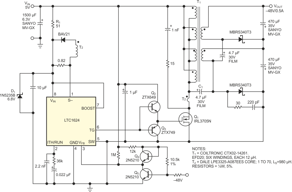
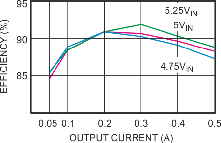
As the demand for networking equipment grows, the need arises for a –48 V supply that can power telecommunication lines. The circuit in Figure 1 delivers 24 W at –48 V from a 5 V input. One of the biggest challenges in this design is choosing the input voltage. Although high-current, 5 V sources are commonly available, lower input voltages generally mean high input currents with accompanying low efficiency. With a relatively simple topology and a 5 V input source, the circuit in Figure 1 delivers greater than 85% efficiency (Figure 2). T1 stores energy during the on-state time of Q1.
 |
||
| Figure 1. | This circuit uses numerous tricks to boost efficiency to more than 85% in converting 5 V to –48 V. | |
Energy transfers to two stacked 24 V outputs to create –48 V. C1 charges to a dc value equal to the 24 V input voltage while clamping T1's leakage-inductance spike and providing a path for input current during Q1's off-state time. This operation results in continuous input current and thus reduces capacitor ripple-current requirements.
 |
||
| Figure 2. | The circuit in Figure 1 delivers greater than 85% efficiency under all conditions and greater than 90% for much of its output-current range. |
|
The reduced input ripple current, which is characteristic of this topology, demands sensing of the switch current rather than the input current. In this case, T2 senses the switch current, eliminating 400 mW of resistor loss without using excessive board space (7×8 mm). Other additions improve the circuit's efficiency and performance. The LTC1624's Boost pin normally provides the internal output driver (the TG pin) with a 5.6 V regulated supply, but TG produces only 4.2 V with a 5 V input. Bypassing the internal regulator by connecting the Boost and VIN pins increases Q1's gate voltage, resulting in a gain of more than 3.2% in overall efficiency. R1 and D1 keep the Boost pin below its 7.8 V rating in the event of an input overvoltage condition. The addition of Q2 and Q3 provides an additional 5.5% of efficiency by speeding transitions and increasing gate voltage from 5 to 5.3 V. This voltage peaking results from excess emitter current as Q2 turns off after charging Q1's gate capacitance. Q4 and Q5 translate the –48 V output to the 1.2 V that the feedback pin (VFB) requires to regulate the output voltage. The LTC1624's switching frequency decreases with output voltage, thereby reducing input current during output short-circuit conditions.