Marián Štofka
EDN
Two amplifiers produce voltages that you can use in a variety of applications.
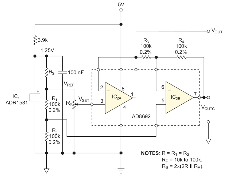
The circuit in Figure 1 generates two analog voltages, which you can vary in a complementary manner. When the straight output voltage rises, the complementary output voltage decreases, and vice versa. The sum of both output voltages is a constant:

where VOUT is the straight output voltage, VOUTC is the complementary output, and VREF is a reference voltage you derive from bandgap cell IC1. You choose the ratio of the resistor divider that connects to the output of IC1 so that the reference voltage is approximately 400 mV. Potentiometer RP sets the desired analog voltage, which connects to the noninverting input of voltage follower IC2A. The output of IC2A provides the straight output voltage, which connects to the inverting input of unity-gain inverter IC2B. The noninverting input of IC2B has a gain of two and connects to the middle of the high-precision resistive divider comprising R1 and R2, which halves the reference voltage. The following equation calculates the output voltage of IC2B with respect to ground:
Thus, the straight output voltage plus the complementary output voltage give the desired constant value equal to the reference voltage.
 |
||
| Figure 1. | The circuit outputs two analog voltages whose sum always equals the reference voltage. | |
You should use either a quad resistor or two pairs of matched resistors for precision resistors R1 through R4. Resistors R3 and R4 form the negative feedback in IC2B, and the other pair of resistors halves the reference voltage. You can omit these four resistors if you use an instrumentation amplifier instead of IC2B. In this case, you must use an RRIO (rail-to-rail-input/output) type of instrumentation amplifier. The output of a contemporary RRIO instrumentation amplifier approaches the low side by a margin of approximately 60 mV, and it would severely degrade the circuit’s accuracy. The output of the Analog Devices AD8692 op amp, however, typically approaches the lower rail by 0.75 mV at a 10-μA load current. The guaranteed value of the margin is 1 mV at this current.
| Table 1. | The results of measuring the voltages at both outputs |
||||||||||||
|
|||||||||||||
The circuit has undergone testing for three values of test voltages: the reference voltage, which represents a fullscale; half the reference voltage; and 0 V. Table 1 lists the measured voltages at both outputs. Any of the output voltages can approach the lower supply rail with an error of less than 0.25% at 400 mV full-scale.