Many applications that use 110 V/230 V-ac mains require a ZCD (zero-crossing-detection) circuit for the ac-line voltage, for example, to synchronize the switching of loads. One method of ZCD uses a high-value current-limiting resistor or a voltage-resistive divider to sense the ac voltage at the controller’s I/O pin. However, depending on whether the I/O pin is in TTL or Schmitt-trigger mode, the ZCD has a delay that depends on the threshold swing of the I/O pin and the slew rate of the power line. For example, assume a 230 V, 50-Hz ac system voltage and a voltage divider of 100 – that is, 230 V/100=2.3 V. Further, assume that the I/O pin triggers at 1 V. This trigger level implies 1 V×100 = 100 V referenced to the 230 V-ac mains. Thus,
100=230×sin(2×π×50×t)
yields a delay of 1.43 msec, which represents 14.3% of the half-cycle period – a significant error.
 |
||
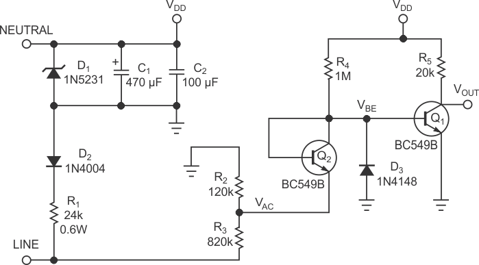
| Figure 1. | This simple two-transistor circuit accurately detects the zero crossing of the input ac mains. | |
Figure 1 shows a low-cost, efficient ZCD using two standard transistors. Coming directly from the ac mains, the supply network comprising C1, C2, D1, D2, and R1 forms a simple half-wave rectifier, which powers the ZCD. Q1 toggles with the ac-mains-voltage ZCD. To compensate for the base-emitter gap, Q2 acts as a diode to block the ac-positive cycle. For efficiency, the detector must sense the ac-mains cycles at as high a voltage as possible. This requirement drives the choice of the transistor. Q2 and Q1, low-noise, small-signal BC549B transistors, have collector-to-emitter-voltage limits of 30 V. With this choice, you must attenuate the ac-mains voltage from 230 to 30 V. (For a BC546 transistor, you can attenuate 230 to 80 V.) Thus, the voltage-divider ratio is 30 V/230 V=13.4%, and the values of the divider resistors are
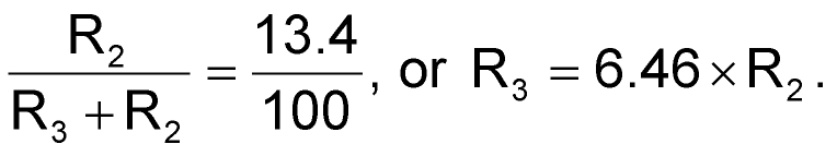
R2 and R3 must be high enough for current limiting. The normalized value of R3, 820 kΩ, means that
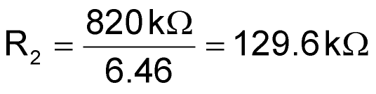
or 120 kΩ, the nearest standard-value resistor. With these values, Q2 can block
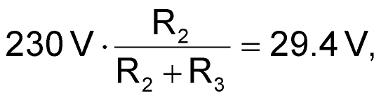
which is less than the transistor’s maximum rating of 30 V.
Upon the ac-positive cycle, the base of Q1 rises to approximately 0.6 V through R4. Q2 acts as a simple diode. So, when the cycle voltage is higher than 0 V, Q2 is reverse-biased and blocks any current flow. At 0 V, Q2 is forward-biased, but it maintains 0.6 V across the base-emitter junction, VBE. Thus, the collector, or base, of Q2, which connects to the base of Q1, stays at 0.6 V. Q1 is saturated for the positive cycle, and the output voltage is low. At the ac’s negative cycle, when the ac voltage is less than 0 V, current flows through Q2. Consequently, the base of Q1, which connects to Q2 ’s collector, falls to less than 0.6 V, which leads to the blocking of Q1 and the output voltage’s becoming high. Note that the base of Q1 can reach about –30 V from Q2; you can add clamp diode D3 for Q1 junction protection higher than –1 V.