This circuit increases the repeatability of noise test setups by providing reference points in the noise-vs.-frequency output generated by the network analyzer. It's based on Maxim MAX4475, MAX427, and MAX4101 op amps.
Noise measurements can be problematic. They often yield a different result with every measurement, even when nothing in the circuit is changing. The test circuit in the Figure 1 minimizes this uncertainty in equipment performance (but not, of course, in the device under test). The circuit does this by providing reference points in the noise-versus-frequency output generated by the network analyzer.
 |
||
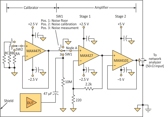
| Figure 1. | This circuit increases the repeatability of noise measurements by allowing users to calibrate the test setup and eliminate the effect of the noise generated by the circuit itself. |
|
The usual setup for noise testing consists of the two-stage amplifier shown in the right side of the figure. Stage 1 boosts the noise of the device under test (DUT) by 40 dB, making the noise associated with stage 2 negligible. The amplifier for stage 1 (a MAX427) was chosen for low noise, both at low and high frequencies. Stage two is a unity-gain buffer (a MAX4101) that provides adequate drive for the analyzer’s 50-Ω input. It was chosen for its low noise and high output drive. A grounded metal cage encloses and shields the entire circuit against electromagnetic interference (EMI).
The reference points are created by first grounding the amplifier input to find the system noise floor and then introducing known levels of noise at the input. These amp inputs are selected by the three-position switches SW1 and SW2.
Position 1 of SW1 provides a noise-floor input to the network analyzer by connecting the amplifier input to ground. Position 2 connects the noise calibrator (a source of known levels of noise), and position 3 connects the DUT for measurements after calibrations are performed.
The calibrator is a low-noise buffer whose input connects (via SW2) to the calibration noise sources – film resistors RA – RC, whose thermal noise can be calculated using:

where k is Boltzmann’s constant 1.38 × 10⁻²³, T is the temperature (300 °K), and R is the resistance.
The buffer (MAX4475) is chosen for its low voltage noise as well as for its very low input current-noise density (0.5 fA/√Hz). This, in turn, makes it possible to connect a large range of resistor values at the input while maintaining a predictable and calculable noise voltage.
Calibrate the system by first setting SW1 to position 2. Install R values whose noise levels are in the DUT’s expected range, and use SW2 to select and measure the noise associated with each one. Divide the noise values measured on the analyzer by the gain of stage 1 to obtain the actual noise at node A. When the measured results correlate with the calculated results, the setup is ready to make measurements. The Table 1 compares the calculated noise with the measured noise for three example resistor values.
| Table 1. | Calculated vs. Measured noise | ||||||||||||
|
|||||||||||||
To make the measurement, connect the DUT by setting SW1 to position 3. The 10-MΩ/ 47-µF RC filter blocks any dc offset included in the low-impedance DUT output.