For a variety of reasons, designers often discover that their creations need yet more power-supply voltages. For example, a system powered by ±2.5 V power supplies suddenly needs a precision –1.4 V reference for a signal-level-shifting circuit and needs a 2.1 V reference to drive an ADC. Your options include adding a couple of operational amplifiers and resistors to level-shift and buffer the system's voltage reference or adding a couple of DACs. Op-amp circuits lack programmability to accommodate design changes, and, although the DACs offer programmability, their settings are volatile, and the outputs are typically unipolar and lacking in drive capability.
The circuit in Figure 1 offers an easy way to generate extra reference voltages and provides a few additional benefits. It allows you to easily generate positive or negative buffered references under software control. Its output buffer sinks and sources as much as 10 mA. You can read and adjust programmed voltages. On-chip storage restores the reference voltages after a power interruption, and a parity bit can indicate a malfunction if an internal device failure accidentally causes the programmed voltage to change.
 |
|
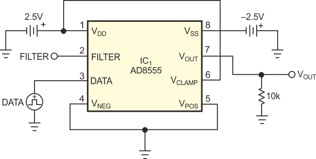
| Figure 1. | Occupying a tiny, eight-lead LFCSP footprint, a programmable instrumentation amplifier doubles as a last-minute adjustable-voltage bipolar-reference source. |
The programmable voltage reference comprises IC1, an Analog Devices AD8555 high-precision auto-zero instrumentation amplifier, which contains an 8-bit DAC as part of its offset-adjustment circuit. In a change from its intended role, the monotonic DAC generates the output voltage, which can swing from VSS (input code 0) to VDD – 1 LSB (input code 255). The DAC's 8-bit resolution provides voltage steps of 0.39% of the difference between VDD and VSS – for example, steps of 19.5 mV with a 5 V supply. The output-voltage, VDAC, temperature coefficient is less than 15 ppm/°C.
The following equation describes the DAC's approximate internal reference voltage, VDAC:
and the following equation yields the circuit's output voltage, VOUT:
VOUT = GAIN(VPOS – VNEG )+VDAC,
in which GAIN represents the circuit's default internal gain of 70 for the differential input. Both inputs connect to ground, and the first term is thus close to 0 V, or 10 µV maximum due to input-amplifier errors, and the circuit's output voltage, VOUT, is equal to VDAC.
 |
|
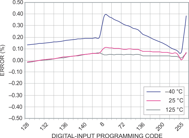
| Figure 2. | Output-voltage error for the reference circuit reaches a maximum of 0.4% at a temperature of –40 °C and a 5 V power supply. |
Until you permanently program the internal registers, they allow you to alter the output voltage and explore the circuit's behavior as a fixed-voltage reference and reprogrammable 8-bit DAC. To program the output voltage, you apply the appropriate pattern according to the first equation and instructions from the device's data sheet. After verification, you can permanently set the output voltage by blowing certain of the device's internal polysilicon-fuse resistors. As Figure 2 shows, for a given output-voltage level, the device's absolute error is less than 0.4% across a –40 to +125 °C temperature range.