The MOSFET power switch is commonly the most vulnerable part of a new switched-mode high-power circuit. One threat for this device is exceeding the value of the maximum allowed pulse current. You cannot exceed this limit, even for pulse durations as short as 10 nsec. You could still thermally damage the MOSFET with a high duty cycle even when the drain-to-source current has a value between the peak and the dc ratings. The FET might eventually enter self-oscillations at a frequency, which might be an order of magnitude higher than your planned operating repetition rate. To protect the FET, you can limit the duty cycle by ac coupling the FET-driver circuit. If you further limit the repetition rate to tens of kilohertz, you needn’t worry about thermal considerations.
 |
|
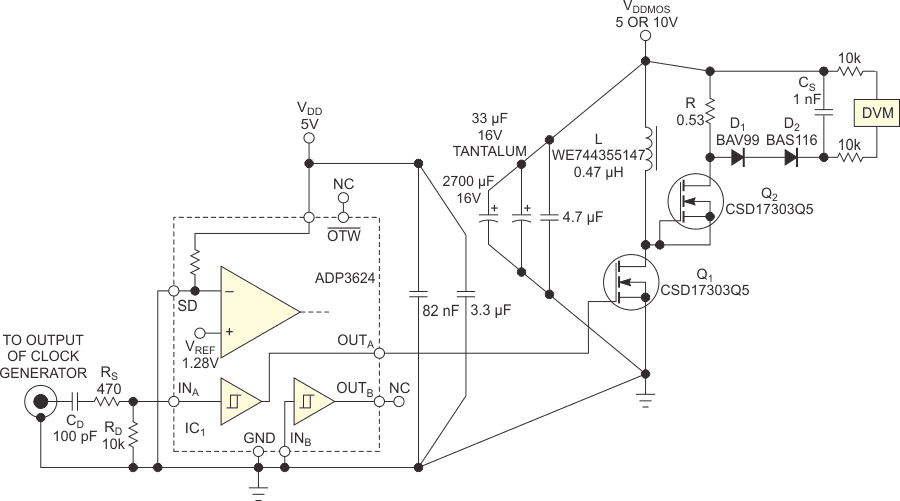
| Figure 1. | The test setup allows you to operate a MOSFET power switch at a fixed turn-on time. The power circuit remains cool with a 10-kHz repetition rate, even at peak inductor currents of tens of amperes. |
To limit the duty cycle of the pulses, use the Schmitt-trigger input of IC1 (Figure 1). You pass the input-voltage waveform through a derivative circuit comprising CD, RD, and RS. The low-to-high transition of the clock causes an abrupt rise of voltage at resistor RD. The output of the noninverting driver therefore goes high. Immediately after this transition, the voltage on RD starts to decrease exponentially. When it falls below VTL, the lower threshold of input INA, output OUTA abruptly falls to 0 V. The time constant (RD + RS + RGEN)×CD yields the rate of exponential decrease. RGEN is the output resistance of the generator of the input clock. You can calculate the value of capacitor CD using the desired pulse width, TP:
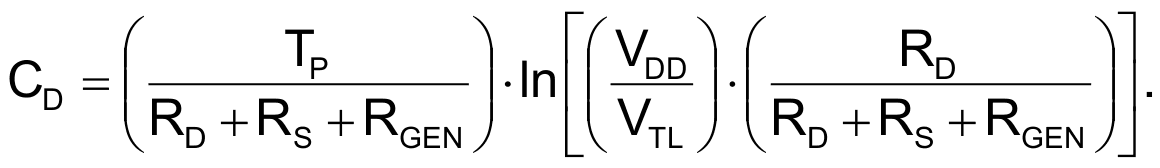
The equation employs an estimate of the value of VTL:

The IC’s data sheet gives the values of 0.8 and 2 V as the limits of the low and high input voltages, respectively. The high-to-low transition of the clock has no effect. This transition causes a sharp negative exponential pulse, which an internal Schottky diode at input INA suppresses. The anode of this internal diode connects to ground, and its cathode connects to input INA. Resistor RS limits the peak current flowing through the protective diode to about 10 mA.
The IC has an output current of ±4 A. The typical on-resistance of Q1 is 2 mΩ. You interconnect Q2’s gate and source pins to create a freewheeling diode. This diode has a typical reverse-recovery time of 33 nsec at a 25 A forward current. When Q1 turns off, the peak inductor current flows through Q2. Voltage VR occurs on power resistor R and is superimposed onto the supply voltage, VDDMOS. The sum of these voltages must be lower than or equal to the manufacturer’s specified value of the drain-to-source voltage of transistors Q1 and Q2.
When testing the circuit, you should monitor the dc-supply current. You can calculate the ideal-case supply current as a function of supply voltage on the power section and the pulse period as follows:

You calculate the pulse width of a single interval when the channel of Q1 is conductive as an approximation relating the rise, fall, on, and off times of the FET:

The sum of differences in the propagation delays of IC1 and Q1 is positive and totals 32.1 nsec. VT is the gate-to-source threshold voltage of Q1. The data sheet gives a typical VT of 1.1 V, and the supply voltage, VDD, has a value of 5 V. These values yield 9.8 nsec for the last term of the preceding equation. TPON is thus larger by 41.9 nsec. For a good design, an ammeter will indicates a supply current one to 1.5 times the ideal value of the current.
You can check the peak voltage at load resistor R. D1 and D2 and storage capacitor CS function as a peak detector. The peak-voltage pulses at resistor R cause a dc voltage at CS of roughly the same value as the peak voltage. You can determine the peak current flowing through the inductor from the voltage at the peak detector using the following equation:

Set the auxiliary supply voltage at 5.078 V, the supply voltage at 10 V, and the clock-pulse repetition frequency to 11,387 Hz. This approach causes the supply’s current to be 0.327 A and the peak voltage to be 16.4 V. The peak current of the inductor reaches 30.94 A. The experimentally determined turn-on time is approximately 1.502 μsec.
The IC driver contributes to the protection of the MOSFETs with an undervoltage lockout. If the supply voltage is on, but the auxiliary supply voltage is off, a voltage could get from the INA pin through internal protective diodes to the VDD pin. The undervoltage lockout disables the control outputs until the auxiliary supply’s voltage reaches a typical value of at least 4.2 V.
The 0.65-mΩ dc resistance of ferrite-core inductor L might seem to be overrated for the circuit. However, the slope of current pulses in the inductor represents a megahertz-range equivalent frequency. The effective resistance at these slopes increases due to the skin effect and the proximity effect. This effective resistance can be many times the dc value.