Examine a traditional Hartley oscillator circuit, and you'll note its trademark: a tapped inductor that determines the frequency of oscillation and provides oscillation-sustaining feedback. Although you can easily calculate the total inductance required for a given frequency, finding the coupling coefficient, k, poses technical difficulties and may require experimental optimization, also referred to as the "cut-and-try" method. This Design Idea presents an alternative equivalent circuit that allows you to model the circuit before building the prototype.
 |
|
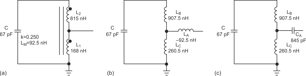
| Figure 1. | A traditional Hartley oscillator’s resonant circuit consists of a tapped inductor and resonating capacitor (a). Allowing for mutual coupling between windings produces an equivalent circuit containing a negative inductance (b). Replacing the negative inductance with a capacitor yields an easily modeled equivalent circuit (c). |
Figure 1 shows the Hartley oscillator's equivalent tuned circuit and component values for an 18-MHz oscillator. The mutual inductance is
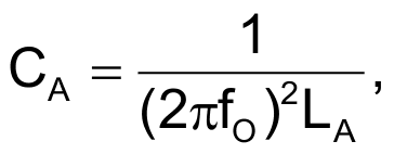
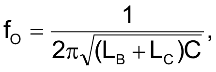
For the equivalent circuit, the equations are:
and
The rest of the equations for the equivalent circuit are:
and
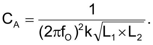
Unfortunately, a truly equivalent circuit requires a negative inductance, LA. However, for frequencies near the resonant frequency f0, you can replace the negative inductor with a capacitor as (Figure 1c), where CA replaces LA. Note that the equivalent circuit's derivation neglects parasitic winding resistances and capacitances.
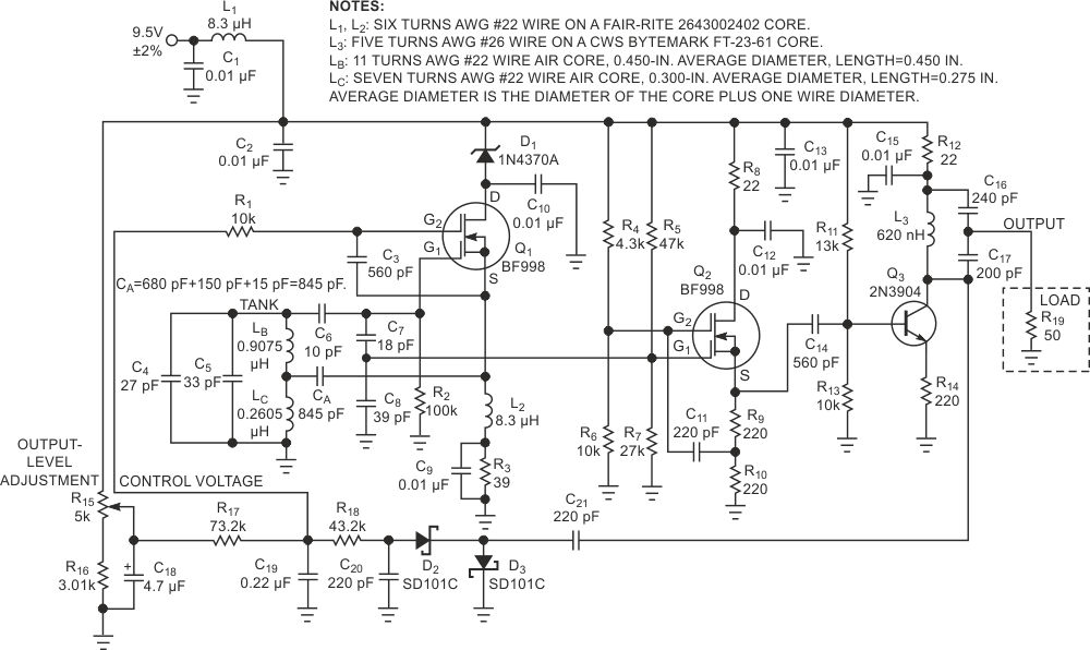
Figure 2 illustrates an oscillator and output buffer using the equivalent circuit. When constructed, the circuit generally performed as expected from an initial Spice simulation. During testing, several components' values required tweaking, and multiple iterations of Spice analysis ultimately yielded the final design.
 |
|
| Figure 2. | This buffered-output, 18-MHz oscillator features a resonant circuit that doesn’t rely on mutual coupling for operation. |
The oscillator's tank circuit consists of LB, LC, C4, and C5, plus the capacitance provided by the voltage divider C6, C7, and C8 – approximately 6 pF, including Q1's and Q2's input capacitances and some stray capacitance. The total tank capacitance of 66 pF approximates the calculated value of 67 pF. Capacitors that connect to the tuned circuit feature ceramic-dielectric construction with NP0 temperature coefficients.
Inductors LB and LC consist of air-core coils mounted with their axes at right angles to each other to minimize stray coupling. However, vibration affects their inductances, and, in a final design, both should consist of windings on dielectric cores or on toroidal cores, providing that the toroids' temperature coefficients of inductance are acceptable for the intended application.
The information in Reference 1 provided basic designs for both inductors, and adjusting the spacing of their turns tuned the oscillator to exactly 18 MHz. For a more rigorous design, you can measure the inductors before installation, but parasitic effects may require some adjustment of the inductors.
The capacitive voltage divider, C6, C7, and C8, applies the proper signal levels to Q1 and Q2. Because the divider's effective capacitance as "seen" by the tank circuit amounts to only 6 pF, you can replace the remaining 60 pF consisting of C4 and C5 with a variable capacitor if the design calls for a tunable oscillator. In this example, the output stage consisting of Q3 and its associated components would require modification to provide more bandwidth if the oscillator requires a tuning range exceeding ±2 MHz.
Capacitor C3 bootstraps Q1's Gate 2 to its source, which provides additional gain and reduces Q1's Gate 1 input capacitance below its already-low value of approximately 2.1 pF (Reference 2). An 8.3-µH inductor, L2, of less than 2 Ω dc resistance connects to Q1's source and presents a relatively high impedance at 18 MHz and provides a dc path from Q1's source to ground through R3. At 18 MHz, L2 has an impedance that consists of an inductive reactance of about 940 Ω in parallel with a resistance of about 3.5 kΩ, which results in a very-low-Q choke. Provided that its inductance and reactance approximate L2's original values, you can substitute a physically smaller inductor for L2. Inductor L1's properties are less critical, but it should present a low Q of 4 to 6 and a dc resistance of approximately 5 Ω or less. You can use a standard-value choke for L1 if it meets these requirements.
Source follower Q2 drives the output stage, which uses a pi-matching network to transform the 50 Ω output load to 285 Ω at the collector of Q3. Bootstrapping Q2's Gate 2 by one-half of the stage's output voltage increases the source follower's gain and dynamic range and reduces its input capacitance.
You can use potentiometer R15 to adjust the circuit's output level from about 0.9 V p-p to approximately 1.5 V p-p across a 50 Ω load. At a constant room temperature of about 23 °C, the frequency remains stable, and the circuitry that controls output level remains stable even with no load on the output. For a fixed-frequency application, the output circuit's loaded Q of 4 provides adequate bandwidth to eliminate retuning of the output circuit for small changes in frequency.
To set the output level to a safe maximum, connect a 50 Ω load to the output, and then adjust the output to 1.5 V p-p. The drain-to-source voltage applied to Q1 will remain at a safe level for all loads from 50 Ω to no load, even though the output-voltage level increases as the load resistance increases. To avoid exceeding Q1's specified maximum 12 V drain-to-source-voltage rating, do not exceed an output-voltage setting of 1.5 V into a 50 Ω load. Note that zener diode D1 reduces Q1's drain voltage to provide an additional safety margin.
In a previous Design Idea, an operational amplifier and a diode-rectifier circuit set the oscillator's gain through a control voltage applied to Q1's Gate 2 (Reference 3). In this design, a simple passive circuit serves the same purpose. A portion of the signal at Q3's collector drives a voltage doubler consisting of D2, D3, C20, and C21. Part of the negative voltage developed by the voltage doubler drives the junction of R18 and C19, the control-voltage node, which also receives a positive voltage from variable resistor R15 through R17, and the resultant voltage sets the output signal level. At start-up, only a positive voltage is present at Q1's Gate 2, and Q1's maximum gain easily starts the oscillator. When the output reaches a steady state, the control voltage reduces and maintains oscillation at the signal level determined by the output level control.
References
- Reed, Dana G, Editor, "Calculating Practical Inductors," ARRL Handbook for Radio Communications, 82nd Edition, American Radio Relay League, 2005, pg 4.32.
- "Practical FET Cascode Circuits, Designing with Field-Effect Transistors," Siliconix Inc, 1981, pg 79.
- McLucas, Jim, "Stable, 18-MHz oscillator features automatic level control, clean-sine-wave output," EDN, June 23, 2005, pg 82.