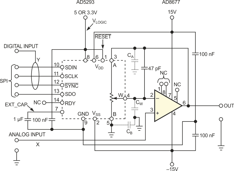
A resistive DAC in a resistive-feedback loop of an op amp lets you create an analog-digital-analog divider. The resistance, RWA, between the W and A terminals of the Analog Devices AD5293 (Figure 1) decreases linearly with increasing the digital-control data, D:
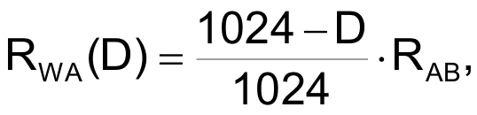
and the value of the RWB, the resistance between the W and B terminals of the DAC, rises proportionally to D as
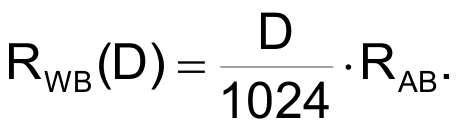
RAB is a constant value of resistance between the ends of the digital potentiometer. The circuit uses resistance RWA as a feedback resistor, and resistance RWB connects between the inverting input of the op amp and ground. The voltage gain of the noninverting amplifier becomes
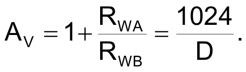
The output voltage is
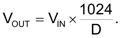
Both the input voltage and the digital-input data can be time variables, and the clock frequency for fetching digital-input data can be as high as 50 MHz.
 |
|
| Figure 1. | The resistive DAC-potentiometer forming the feedback for an op amp controls the op amp’s gain as inversely proportional to the digital-input-data word. The circuit thus becomes a two-quadrant divider. |
The potentiometer's data sheet provides the ground-referred parasitic capacitances at the A, B, and W terminals of the potentiometer. Thorough measurement of the capacitances at these terminals provides enough data to determine capacitances between the terminals. An evaluation of the measured data shows that the direct capacitance between the A and W terminals at the midscale position of the wiper is just 2.4 pF:

If you assume that the five segments of the potentiometer are ordered topologically into a chain, then the direct intercapacitance between the A and B ends of potentiometer is

The capacitance per segment of the five segments of the potentiometer is
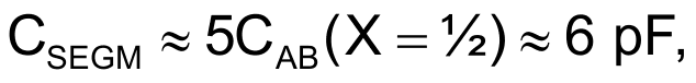
where X = ½ denotes the midscale of the resistive DAC.
The five-step distributed RC line of the potentiometer has a time constant of

where RAB is 20 kΩ. The ground-referred wiper capacitance, CW, of 40 pF is much higher than the intercapacitances and creates a time constant:
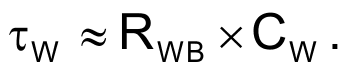
The feedback network of the amplifier is frequency-compensated for τSEGM ≈ τW. Thus, you can calculate the value of RWB as 600 Ω, meaning that the voltage gain of the amplifier, AV, is 32.3. For gains higher than 32.3, the effect of CW becomes negligible, and you need not bother about amplifier stability. To suppress the derivative behavior of the amplifier for gain values of two to 32.3, you can add a 40-pF compensating capacitor in parallel to feed back part of the potentiometer. The amplifier thus has an integrating character for all gains down to a value of two.
You fetch the divisor, Y, which is a digital-data word, D, through a standard SPI (serial-peripheral interface). After power-on, you must initially neutralize the write-in protection of the resistive DAC. You have to first program the control bit C1 to the value of one, whereas it is zero by default. You achieve this task by clocking in the word containing C3, C2, C1, and C0, which equals 0110, and you put the desired C2 and C1 values at data positions D2 and D1. After performing these steps, you change the wiper position in which the control bit is C3, C2, C1, and C0, which equals 0001, and the data bits, D9 to D0, represent the gain as 1024/D.