Figure 1’s circuit achieves a wider dynamic range and higher output frequency than any commercially available voltage to frequency (V-F) converter. Its 100 MHz fullscale output (10% overrange to 110 MHz is provided) is at least ten times faster than available units. The circuit’s 160 dB dynamic range (8 decades) allows continuous operation down to 1 Hz. Additional specifications include 0.1% linearity, 250 ppm/°C gain temperature coefficient, 1 Hz/°C zero shift, 0.1% frequency shift for VSUPPLY = 5 V ± 10% and a 0 V to 5 V input range. A single 5 V supply powers the circuit.
A1, a chopper stabilized amplifier, servo biases a crude but wide range core oscillator in Figure 1. The core oscillator drives a charge pump via digital dividers. The averaged difference between the charge pump’s output and the circuit’s input appears at a summing node (Σ) and biases A1, closing a control loop around the wide range core oscillator. The circuit’s extraordinary dynamic range and high speed derive from core oscillator characteristics, divider/charge pump-based feedback and A1’s low DC input errors. A1 and the LTC6943-based charge pump stabilize circuit operating point, contributing high linearity and low drift. A1’s low offset drift allows the circuit’s 50 nV/Hz gain slope, permitting operation down to 1 Hz at 25 °C.
 |
|
| Figure 1. | 1 Hz to 100 MHz V-F converter has 160 dB dynamic range, runs from 5 V supply. Input biased servo amplifier controls core oscillator, stabilizing circuit’s operating point. Wide range operation derives from core oscillator characteristics, divider/charge pump-based feedback and A1’s low DC input errors. |
The positive input voltage causes A1 to swing negatively, biasing Q1. Q1’s resultant collector current ramps C1 (trace A, Figure 2) until Schmitt trigger inverter I1’s output (trace B) goes low, discharging C1 via Q2. C1’s discharge resets I1’s output to its high state, Q2 goes off and the ramp-and-reset action continues. D1’s leakage dominates all parasitic currents in the core oscillator, ensuring operation down to 1 Hz. The ÷64 divider chain’s output clocks the LTC6943-based charge pump. The charge pump’s two sections operate out-of-phase, resulting in charge transfer at each clock transition. Charge pump stability is primarily determined by the LT1460 2.5 V reference, the switches low charge injection and the 100 pF capacitors. The 0.22 μF capacitor averages the pumping action to DC. The averaged difference between the input derived current and the charge pump feedback signal is amplified by A1, which biases Q1 to control circuit operating point. Core oscillator nonlinearity and drift are compensated by A1’s servo action, resulting in the high linearity and low drift previously noted. A1’s 1 μF capacitor provides stable loop compensation. Figure 3 shows loop response (trace B) to an input step (trace A) is well controlled.
 |
|
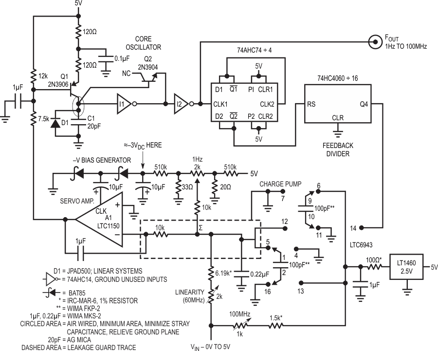
| Figure 2. | V-F operation at 40 MHz. Core oscillator waveforms viewed in 670 MHz real time bandwidth include Q1 collector (Trace A) and Q2 emitter (Trace B). Ramp-and-reset operating characteristic is apparent; reset duration of 6ns permits 100 MHz repetition rate. |
Some special techniques enable this circuit to achieve its specifications. D1’s leakage current dominates all parasitic currents at I1’s input; hence Q1 must always source current to sustain oscillation, assuring operation down to 1 Hz. The 100 MHz full-scale frequency sets stringent restrictions on core oscillator cycle time. Only 10 ns is available for a complete ramp-and-reset sequence. The ultimate speed limitation is the reset interval. Figure 2, trace B, shows a 6 ns interval, comfortably within the 10 ns limit.
A scaled resistive path from the input to the charge pump corrects small nonlinearities due to residual charge injection. This input derived correction is effective because the charge injections effect varies directly with input determined frequency.
 |
|
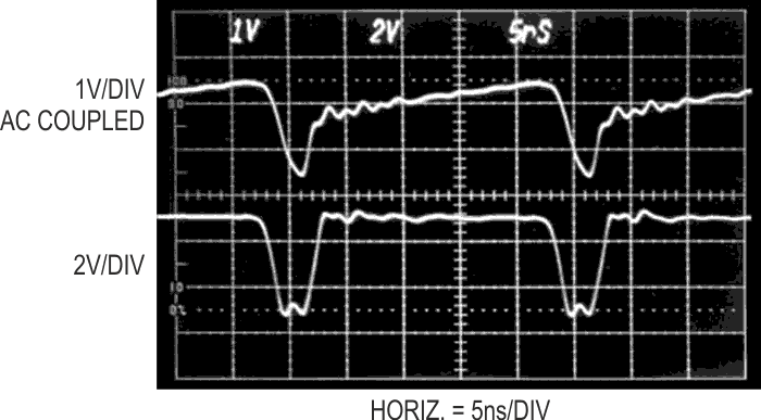
| Figure 3. | Response (Trace B) to an input step (Trace A) shows 30 ms settling time at summing junction (Σ). A1’s 1 µF capacitor shapes response, stabilizing feedback loop. Clamped response on negative going input step is due to summing junction limiting. |
Prototype and small lot construction may proceed using the schematic and its notes, but component selection should be considered for volume production. Table 1 lists applicable components and their selection targets.
| Table 1. | Selection criteria for components ensure V-F performance. First five entries enhance operation below 100 Hz. Last entry assures reliable feedback divider operation. |
||||||||||||||
|
|||||||||||||||
To calibrate this circuit apply 5.000 V and trim the 100 MHz adjustment for a 100.0 MHz output. Next, ground the input and adjust the 1 Hz trim for 1 Hz output. Allow for long settling time, as charge pump update rate at this frequency is once every 32 seconds. Note that this trim accommodates either offset polarity because of the –V bias derived from A1’s clock output. Finally, set the 60 MHz adjustment for 60.0 MHz with 3.000VIN. Repeat these adjustments until all three points are fixed.