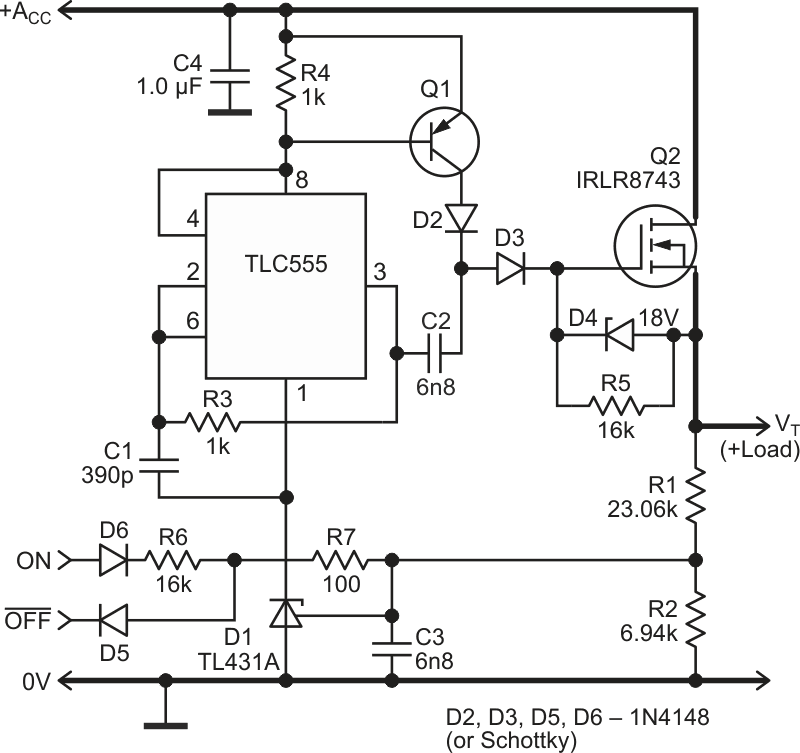
Many rechargeable battery types can be damaged by deep discharge. This Design Idea circuit performs under-voltage protection (UVP) to prevent this, as well as acting as a load switch (Figure 1). With little or no modification, it can work for almost any battery type, with voltage from 4.5 V – 19 V. Standby current is under 1 µA.
 |
|
| Figure 1. | The circuit is set up for a 12 V lead accumulator with gelled electrolyte at 20 °C. Another type of accumulator may require component value changes. |
High-side N-channel MOSFET Q2 reduces cost compared to a P-channel part. Turn-on and -off are inherently soft, so switching spikes are avoided.
Operation
The first time the battery/accumulator is connected to +ACC, the circuit is off. C3 is discharged, so the programmable reference TL431A (D1) will be off, with leakage under 1 µA. Thus, all other elements of the circuit are disabled, and Q2 is off because its gate is discharged through R5.
In this state the circuit is waiting for an enabling positive pulse at the ON input – via a button or other controller. During this pulse, the TL431A turns on, providing power to the TLC555, configured as an oscillator. Through C2 & D3, the oscillator produces a bootstrap voltage on the gate capacitance of Q2, turning it on.
After the ON signal is removed, the circuit remains in the active state because the voltage from divider R1-R2 charges C3, maintaining the loop from D1 to Q2 back to D1.
The circuit disconnects the load and turns itself off if the /OFF input goes low or the under-voltage trip point is reached.
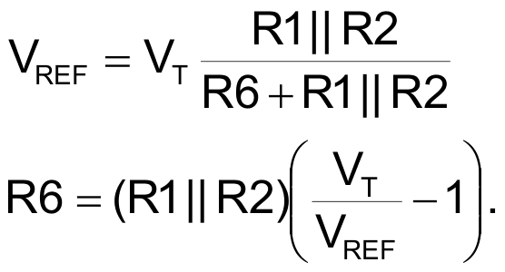
The trip point expression is:
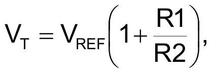
(VREF is the TL431 2.5 V reference voltage)
So
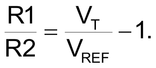
To make the influence of IREF (4 µA max.) negligible, make the current through the divider at least 100 times IREF:
R1 + R2 = 30 kΩ.
So for a trip point of 10.8 V, the calculated values are:
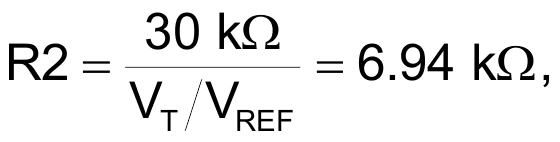
R1 = 30 kΩ – R2 = 23.06 kΩ.
The TL431A has a VREF tolerance of 1%, so tolerances of R1 and R2 should be better to minimally degrade the trip point accuracy, or a trimpot could be added.
As a matter of good practice the current IREF should be less than half of its absolute maximum rating of 10 mA. Hence:
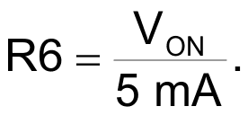
The upper limit of R6 is defined by:
So,
R6 = 17.8 kΩ.
If you select R6 near this limit, you can prohibit any attempts to switch on the load while the accumulator is depleted. The /OFF input has priority over ON.
Battery voltage monitoring takes place after switch Q2, so a low RDS(ON) is essential for correct operation.
With a high load current, the switching times should be minimized to reduce power dissipation. For a quick charge of Q2’s gate capacitance CG during turn-on, oscillator frequency should be high (it’s about 900 kHz here). For quick turn-off, R5 should not be too high: the time depends on R5 × CG.
Q1 prevents connection of Q2’s gate to +ACC through D2 & D3 when the circuit is disabled. Any PNP transistor with a moderate gain (30-150) can be used (e.g., 2N2904). Transistors with higher gain (e.g., BC556-BC560) may require R4 reduction to ensure Q1 is off during the circuit’s off state. Q1 though should be reliably turned on by the current through the 555; working near its upper frequency limit and using a low R3 value ensures enough R4 drop.
Low power Zener diode D4 should be spec’d for VGS(MAX) of Q2.
The choice of Q2’s main parameters is system-dependent. Because CG is used as a filter capacitor, attention should be paid to it too. Adequate values lie in the 2 nF – 10 nF range; greater capacitance may require C2’s value be increased. As a rule of thumb, C2 can range from CG to 2CG. The value of C2 has an influence on the turn-on time.