Hugo Letourneau, Future Electronics
True audiophile electronic designers have always dreamed of designing the best amplifier perfectly reproducing the recorded soundstage. They may have started to dream about it when they learned in their first electronic classes that the class-A topology gives exceptional results in terms of linearity. There is sometimes a passionate student who will try to reinvent the wheel despite the warning of his teachers and commit himself to design a 150W/channel Class A amplifier to impress the whole class with powerful and perfect sound. And every time the design reaches the final stage, it is always fun to see that the amp is mostly a powerful heater for the cinema room, the casing of the amp being a big hot heat sink for the output stage transistors!
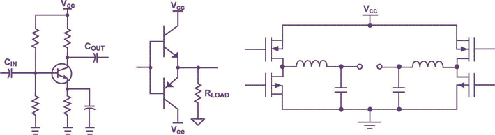
This kind of passionate student will usually pursue another lowest power design, potentially using class B or AB, or if the student is patient enough to do research on the various topologies, class D. For the neophyte to amplifier design: in class A systems the output stage transistors are working on 360 degrees of the signal where in class B, 180 degrees only. For class AB, the transistors will work on 180 to 270 degrees approximately, all depending on the quiescent current of the output stage. Class D amplifiers are often referred to as being “digital” amplifiers because the output stage is working with only fixed high and low voltage values, generating a square wave to feed the speakers through filters. The main advantage of Class D topology is its efficiency that can get in the high nineties of percents due to its digital nature. Figure 1 shows typical circuits for each output stage topology.
 |
|
| Figure 1. | Typical basic circuits for Class A, B or A/B and full bridge Class D amplifiers respectively. |
Class D audio amplifiers have been around for digital sources, more than 25 years, but only gained popularity over the past 10-15 years or so. They were mainly used in low frequency application and high energy demands of subwoofers due to their high efficiency, but very rarely for medium or high frequencies, due to the high distortion caused by a lack of performance of the technology that was just not made for this kind of precision switching activity at that time.
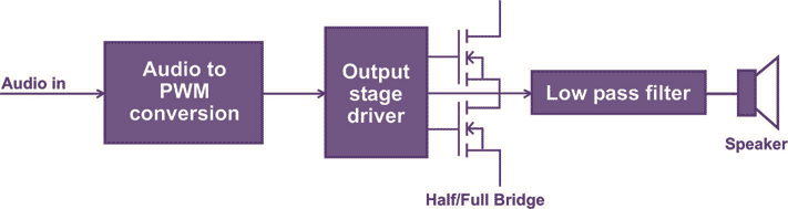
Many parameters have to be taken into consideration before getting to a decently audible class D amplifier. Each element of the signal chain must be adequately controlled to achieve a good audio signal through the whole audible frequency range. Figure 2 shows a simple typical signal chain block diagram for digital amplifiers. Every single detail will have to be adjusted to reach a certain balance that satisfies the ear.
 |
|
| Figure 2. | Class D signal path block diagram. |
Analog PWM Conversion Stage
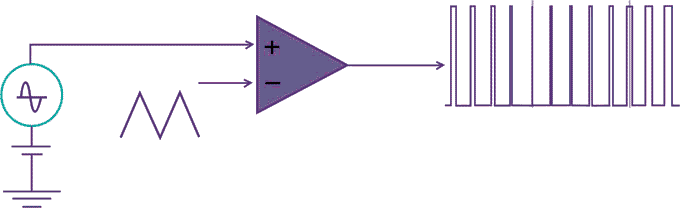
The PWM signal can be generated by an analog or a digital circuit, just like the audio source can be analog or digital. PWM is easily achieved in analog by comparing a triangular waveform to the audio signal, as seen in Figure 3. For digital sources, PCM can be converted into PWM using a DSP processor. In any case, the jitter and stability of any oscillator used for the PWM is of primary importance, as a few pico seconds RMS of jitter will make the dream of getting 100dB+ of SNR out of reach. In digital PWM systems, quantization error is added on top due to the finite amount of PWM steps.
 |
|
| Figure 3. | Simple signal-to-PWM conversion. |
Several digital noise shaping techniques have been developed over time, such as pulse density and delta sigma modulation, which theoretically allows the noise power to be pushed higher in frequencies outside the frequency band of interest where the filter will attenuate it better.
If a comparator will be output with high slew rate the LMV7239 which has used, a totem pole is preferred, such as a 45ns propagation delay, 1.2ns rise/fall times. The quality of the layout will be critical to avoid any ringing, and the power distribution and decoupling have to be taken care of meticulously to avoid further jitter in the output waveform. Excessive capacitance should also be avoided along the output signal path leading to the MOSFET driver.
Single-ended vs. Differential
Prior to selecting if the output stage will be single- ended or differential, it is important to understand what impact this choice has on the design. A single-ended mode is more cost effective since fewer parts are necessary, but it will require a coupling capacitor to avoid the DC offset to flow current into the transducer. The variations from the supply voltage will inevitably be directly transferred to the output, further increasing the distortion level. In single-ended mode, closing the loop on the output will be necessary.
The differential approach costs more but also brings many advantages such as lower even harmonic distortion, increased immunity to power supply variations, reduced power dissipation in each transistor, and better control of DC offset without the need for coupling capacitors. While closed- loop operation can improve the output signal, differential topology will allow open loop operation with much less signal degradation compared to single-ended operation.
Output MOSFET Stage and Driver
While all the stages along the signal path are important, the 2 parts that are the most intimately tied to the signal output quality are the MOSFETs output and their driver. The quality of the sound will greatly depend on the quality of the pulse train and mostly each difference from an ideal PWM signal will further degrade its quality.
For this stage, many characteristics are important and must be considered: drive current and MOSFET input capacitance, dead time to avoid conduction overlap, on resistance but also turn on/off time of MOSFET. All of these parameters might also impact the power dissipation of the output MOSFETs. The dead time is the delay between the turn off of one MOSFET and the turn on of the other MOSFET, time during which both MOSFETs are off (or in progress to the off state). If no dead time is inserted, as a MOSFET is turning on, the other MOSFET will most likely still be conducting and a current will flow from the positive supply rail to the negative supply rail, directly through the two output stage MOSFETs. This current is called the shoot-through current and must be minimized by adding a proper dead time. It is considered as being the main cause for non-linearity in class D audio systems. A small dead time in the order of a few tens of nanoseconds may degrade the THD to above a percent. The MOSFET selection of and the symmetry of each push-pull branch is a critical factor to a decent amplifier.
A proper MOSFET drive current must be selected with respect to the MOSFET stage input capacitance in order to generate sharp rising and falling edges on the gate which will in return provide sharp edges on the main output signal, also soliciting the main supply rails with a wideband pulse train.
Power dissipation and choosing the right MOSFET
A class D switching stage will ideally spend the vast majority of its time either high or low in full conduction mode. The transistors being saturated, the power dissipation is kept to a minimum. As seen in Figure 1, the typical class D system uses a push-pull switching stage, either in a half or full bridge configuration, where the output signal is a square wave, where the conduction time is split between the upper rail MOSFET and the lower rail MOSFET which could theoretically be N and P channel but dual N channel is preferred for increased symmetry and better dead times. When turned on, the MOSFETs are ideally exhibiting low voltage drops as a function of their respective RDS(ON) and will only dissipate a minimum of power. This advantage is enormous not only because it could save power but especially for the enormous size savings. By comparison, a 100W class A output stage would generate an enormous 300W of heat dissipation, requiring very bulky transistors and heat sinks, class AB could go well by using TO3 transistors with conveniently sized heat sinks, while the class D amplifier show a definite advantage by perhaps getting away with an SOT223 or TO89 sized casing for its output transistors. A good power amplifier can therefore be packaged in a relatively small size. With the ever evolving technology, there is virtually no limit to the efficiencies and sizes reached with class D systems.
One common pitfall is to take for granted the high efficiency since circuit designers will naturally tend to select the lowest MOSFET and expect it RDS(ON) to run perfectly cool. The reality can be quite different.
Choosing the lowest RDS(ON) comes with some drawbacks, as the input parasitic capacitance will be high. An increased input capacitance also means it is much harder to drive, this could limit the switching frequency, affecting the rise and fall times. One should try to limit the input capacitance for a better control of the MOSFET. Generally, among MOSFETs with low RDS(ON), as the input capacitance is decreasing the drain- source breakdown voltage decreases as well. The optimal MOSFET would then be the one which has approximately the right drain source breakdown voltage VDSS, with an acceptable RDS(ON) for acceptable power losses but also to minimize the input capacitance in order to achieve a tight switching while relaxing the output drive constraint on the MOSFET driver.
A designer should not neglect the dissipation incurred by switching losses which are caused by the capacitances of the discrete device. The total power dissipated in each MOSFET can be expressed as follows:
PD = PRESISTIVE + PSWITCHING = RDS(ON) × ILOAD2 + (CRSS × V2 × FSW × ILOAD) / IGATE
For example, for 100W output stage MOSFET, let’s assume we chose the FDP047N10, a great MOSFET from Fairchild Semiconductor with an RDS(ON) of 3.9mΩ and a CRSS of 455pF, driven by a 1A MOSFET driver stage and driving an 8Ω load with a swing voltage of 50V peak at 100kHz, will exhibit a power dissipation not exceeding:
PD = 0.0039×5A + (455×10–12×502×100×103×5A) / 1A = 0.0195 + 0.568 = 0.588W
By selecting the FDP3651U from Fairchild, with an RDS(ON) of 0.018Ω max and a CRSS of 89pF, the power dissipation then becomes:
PD = 0.018×5A + (89×10–12×502×100×103×5A)/1A = 0.09 + 0.111 = 0.201W
We can conclude that the choice of a MOSFET should not only be based on on-resistance but also based on an optimization of an ensemble of characteristics.
A good complement to the FDP3651U, is the MOSFET driver LM27222 from National Semiconductor with its adaptive shoot-through protection which could potentially help to reduce the dead time down to an interesting 10ns with an appropriate choice of MOSFETs, allowing down to 30ns minimum pulse width.
Output Filter
Once the designer has gone through the output bridge design, the hard work is not over yet. Another critical stage requiring design efforts is the filter stage. This stage’s purpose consists of eliminating the switching and reducing the bandwidth down to the useful part of it, mainly letting through the audible part of the signal up to 20kHz. Some designers will rely on the speaker’s natural ability to filter the high frequency content, but the resulting transfer function is then greatly speaker dependent. A serious designer will most likely use a passive filter for which the components will be carefully selected. Generally a 2 poles low pass transfer function is desired, such as Butterworth, Bessel or Gaussian. The ideal audio filter transfer function will avoid non-linear phase shifts and have a constant group delay in the frequency band of interest while having sufficient attenuation at the switching frequency.
Since the filter will carry high current and high dI/dt, the coil will be selected in order to minimize the audible distortion caused by non-linear effects when its core is getting closer to saturation, while having a self resonant frequency that is higher than the switching frequency and a few of its harmonics to avoid parasitic self resonance and maximize attenuation of the high switching activity. The choice of capacitors is really important as well. One will avoid aluminum electrolytic capacitor and will prefer either Teflon, polystyrene, polycarbonate or even polypropylene or mylar. Some of these exotic films can be quite expensive but will prevent too much sound coloration compared to aluminum electrolytic.
PCB
One must take care in ensuring a proper layout as parasitic inductance of the signal traces, especially the ones carrying the output current, can generate ringing, which is greatly unwanted. The switching nature of class D amplifiers will produce high dI/dt that will result in voltage drops in parasitic elements and perhaps ringing as well. To help control this phenomenon, snubber circuits can be added at the output and the rise time can be adjusted to the frequency content to avoid exciting the resonating circuit. These solutions are mostly considered as patches to overcome the ringing problem and will most likely further degrade the audio signal and will never be as good as a proper layout that minimizes signal path characteristic impedance variations, controls parasitic elements and a proper component selection by taking this potential problem into account.
Next, the power distribution, filtering and decoupling are critical to maintain low noise stable voltage rails at all time especially in a single ended half bridge configuration where all the variations below the cutoff frequency will be passed along to the speaker. Many other parameters should be taken into account but this article should nonetheless provide a good base for a strong design. A good audio system design is the fruit of several months of work in which the path is full of compromises and hurdles, but succeeding is certainly among the most rewarding experiences, involving your senses and emotions for an unforgettable moment.