When EDN debuted in 1956, it began to provide technical information to electrical and electronics designers as transistors began to change the industry. Take a look at these electronics developments and ideas from technical/white papers from that era, and read part 1 of this series for more technology and events from this pivotal time.
Germanium rectifiers for industrial applications1
In the process of getting DC power from an AC source, metallic rectifiers were the device of choice in 1956 in the field of AC to DC conversion. Magnesium copper sulphide, copper oxide, and selenium were the materials that were typically used for these devices. Around 1956, germanium was being looked at seriously as a rectifier material. The germanium rectifier had different characteristics which led to an effort for new design techniques to be developed.
Selenium and copper oxide rectifiers had large rectifying areas, operated at low current densities of 0.3 ampere per square inch. This necessitated the use of large cell areas or stack assemblies to provide for large power supplies. As a bonus, the large area provided a perfect way to dissipate the heat where it is generated as well as providing a large heat sink or thermal capacity to take care of sudden current surges or short-time overloads. Voltage surges were also taken care of easily as long as they did not last for a long period of time. Designers were comfortable with these devices and they had been used successfully for many years.
The newer germanium rectifier was quite a bit smaller and operated at several hundred amperes per square inch of current density. However, it proved to be much more efficient, which resulted in less heat to dissipate in total but still a large amount on a unit area basis (Figure 1). The germanium crystal itself was a small wafer, 0.020” to 0.030” thick and up to 1” in diameter, but most of the rectifiers for power applications used a crystal about .5” in diameter.
 |
||
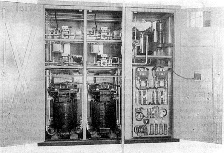
| Figure 1. | Germanium rectifiers used in a single cubicle rated at 60 volts and 2,000 amperes. (Image courtesy of Reference 1). |
|
The basic advantages and disadvantages of the selenium rectifier were as follows.
Advantages
- High operating efficiency
- Very good regulation
- Small size
- Low forward resistance
- High reverse resistance
Disadvantages
- Low thermal capacity
- Temperature limitations
- Susceptibility to current surges
- Susceptibility to voltage surges
Engineers came up with creative and effective ways to counter the disadvantages.
Stagger-tuned transistor video amplifiers
In the paper “Stagger-tuned transistor video amplifiers,” (Reference 2) author Victor H. Grinich speaks about video amplifier design for TV and RADAR in 1956 where tight control of the gain function was not needed. Designing this type of a video amp with vacuum tubes was pretty easy back then. Back then filter amplifiers using grounded cathode vacuum tubes was a hot topic in design architectures.
Since transistor design was still early but finding its way into so many designs to replace vacuum tubes, designers considered them for video amps. The difficulty was that transistors, at that time, were more complex (bi-lateral) than vacuum tubes in these types of circuits, and simple vacuum tube type of methods did not easily apply to transistors.
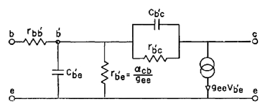
In 1956, Georg Bruun developed a design architecture for common emitter amps that was pretty straightforward (Reference 3). The key stumbling block here with transistors to be used in a video amp design was the difficulty due to bilateralness in the transistor. Bruun circumvented this by lumping the Miller capacitance, which is the capacitive part of the Miller effect produced by the collector barrier capacitance, with the diffusion capacitance. This lumping enabled simple and accurate design procedures for video amplifiers.
 |
||
| Figure 2. | Here is a hybrid-pi common-emitter stage two-port representation. The Cb’c (Cc) capacitance is the primary reason that transistors were not able to work well in a video amplifier design. (Image courtesy of Reference 3). |
|
Grinich applied Bruun’s method to the design of a Butterworth maximally-flat stagger-tuned video amp architecture (Figure 2).
Closed circuit TV in hospitals
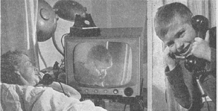
Many hospitals in 1956 did now allow visitors under 14 years of age. In response to that need, engineers developed the “Visit-Vision” system that allowed a visitor in the lobby to speak by phone and even allow the patient and caller to see each other on the TV screen in the hospital room. A standard 60-B camera and a 602 monitor were inside a triangular booth sized 6 feet on a side. A telephone was placed at the booth, fluorescent lights were placed in the booth for illumination, and the camera’s output signal was fed through the monitor to the main distribution point of the hospital's television distribution system. It can be fed into an unused channel or, in 1956 in Chicago, channels 2, 5, 7, 9, and 11 were being used, so the Visit-Vision signal was sent through the hospital distribution system on channel 3-1/2 so that the double side-band signal could be transmitted without cross talk problems (Figure 3).
 |
||
| Figure 3. | Shown here is the “Visit-Vision” system being used by a patient at Morristown Memorial Hospital in NJ. She is talking to her young son who appears on a monitor at her bedside. (Image courtesy of the “Of Current Interest” publication in 1956). |
|
This system was developed by ITV, Inc., a New York distributor of closed-circuit TV equipment that was manufactured by the Dage Television Division of Thompson Products, Inc., Michigan City, IN. The unit came complete with a self-contained camera, monitor, and special booth, with a cost of about $2,500.
Millimeter waves and their applications4
In 1956, R. G. Fellers discussed the frequency region between that era’s radio spectrum and the Infrared region known as the millimeter wave range because its wavelengths spanned 1 mm to 10 mm (Reference 4). This translates into frequencies from 30,000 Mc to 300,000 Mc or 30 GHz to 300 GHz as we know it today. The lower limit of this frequency range was just a bit above radio frequencies used during World War II and the upper limit was the maximum frequency for that era’s known microwave designs.
In 1956, many new military, as well as civilian, needs were emerging for the existing spectrum that was filling up fast. Higher bandwidths were also needed for existing services. The millimeter wave spectrum was seen as a way to accommodate the new services and relieve the pressure on the existing frequency spectrum being used. The millimeter wave spectrum represented a 10× bandwidth capability than the current usage in 1956. The reasons for increased use of short pulses and other wide-band modulation in television, RADAR, and communications systems demanded large bandwidth and higher carrier frequencies.
Other advantages in the millimeter wave region were smaller antenna sizes at these wavelengths and more narrowly focused beam width enabling higher gains (a 10 mW transmitter power yielded an effective radiated power of 1 kW).
One disadvantage was the atmospheric effects at millimeter wave frequencies. This made the use of millimeter wavelength equipment difficult in bad weather (clouds, fog, rain, etc.), however, these properties made this wavelength range a very good choice for cloud and rain detection RADAR uses. In communication usage, distances were very limited at that time.
Another key usage of this spectrum was microwave spectroscopy, which was used in the investigation of molecular structures. In 1956 it was also believed that the transition from the conducting to the superconducting region might occur in this millimeter wave range region for use in this field of research.
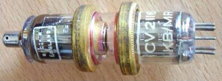
There was great hope for klystrons, magnetrons, and traveling wave tubes (TWT). Reflex klystrons, at that time, had been developed in the frequency range from 26,000 to 60,000 mc, with power outputs from 30 mW at lower frequency limits down to 5 mW at 60,000 mc. These power levels at that time were useful for most local oscillator and measurement applications and were thought to represent almost the ultimate in klystron development. Klystrons used at 60,000 mc needed close tolerances, excellent surface finishes, and complex fabrication techniques (Figure 4).
 |
||
| Figure 4. | The reflex klystron CV2116. (Image courtesy of Roy Johnson’s private collection). |
|
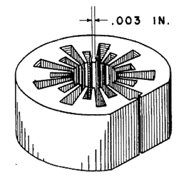
Pulsed magnetrons were shown to be better for short-wavelength use. Peak power levels of 100 kW at 6.3 mm and 20 kW at 3.3 mm were achieved in 1956. Detectable power was observed at 1.1 mm. These tubes have mostly used the rising-sun anode structure, which is constructed with extremely thin vanes (Figure 5).
 |
||
| Figure 5. | This is a rising sun anode structure (made with very thin vanes) in a millimeter wave magnetron. (Image courtesy of Reference 4). |
|
Finally, traveling-wave amplifiers using helix and waveguide structures were shown to deliver 10 mW of continuous wave (CW) power at 5 mm. Backwards wave oscillators (which today can reach the Terahertz region) were designed as structures of the helical and space harmonic type and were operated at wavelengths of 3.0 mm. It seemed that tubes of this type proved to have the greatest promise for further expansion into the higher frequency spectrum.
References
- Germanium Rectifiers for Industrial Applications, L W Burton, AIEE, March 1956
- Stagger-Tuned Transistor Video Amplifiers, Victor H. Grinich, IRE Transactions on Broadcast and Television Receivers, 1956
- Common-Emitter Transistor Video Amplifiers, Georg Bruun, Member IRE, 1956
- Millimeter Waves and Their Applications, R. G. Fellers, Member AIEE, October 1956