Joseph Sawicki, Executive Vice President for IC EDA at Mentor, a Siemens Business
Electronic Design
Artificial intelligence (AI) has proven useful in a range of applications, even in the electronic-design-automation arena. And by the looks of things, AI will have a greater impact on EDA technology this year.
As the adoption and sophistication of artificial-intelligence (AI) technology continues to expand, it’s increasingly clear that AI and its many derivatives (deep learning, machine learning, etc.) will lead to profound socioeconomic changes of a magnitude the world hasn’t seen since the industrial revolution. While it can sometimes be a controversial topic in terms of its ethical vs. unethical use, and potential impact on global socioeconomics, one thing is certain: AI is, even in its infancy, being effectively deployed to vastly improve and better automate a number of tasks ranging from data collection, communications, robotics/factory automation, automotive design – and to even our own small but mighty industry, EDA, in chip design.

In short (and excuse the mixed metaphor), the genie is out of the bottle, and we need to embrace it. In 2020, we can certainly expect to see continued growth in the design and deployment of AI chips and systems.
To help companies deliver more sophisticated AI technologies, EDA companies such as Mentor, a Siemens business, are doing two things:
Developing tools to help companies design AI-accelerators faster.
- Leveraging machine-learning algorithms to improve IC design tools so that they can deliver better results for customers faster.
- Let’s take a closer look at these.
Tools for Better, Faster AI/ML design
Most AI starts out as a mathematic algorithm. The developer creates the algorithm in a math tool, translates it to C code, and then runs that algorithm on a processor. Inevitably, they’ll find that parts of the algorithm run optimally, while other parts run more slowly.
That’s why there’s a vast rise (and subsequent investment from the venture community as well as from large corporations) in AI/ML accelerator IP and silicon development. Some algorithms can be forced (by tweaking the C code) into running on existing AI ASSP architectures with performance and power compromises, but others (think of mobile devices, for example) require dedicated logic to run optimally.
Developing the right AI architecture for a given application screams for EDA tools that enable companies to work with higher levels of abstraction. We’re starting to see increased business in our Catapult HLS (High Level Synthesis) technology for companies developing AI IP accelerators for their system-on-chip (SoC) designs. This enables AI architects to develop their math code, translate it to C or SystemC, and see upfront which parts of their algorithm should be implemented in hardware vs. software. They can then converge on the ideal architecture much sooner than trying to go down to the RT level right away.
When they do on the ideal architecture and select the hardware configuration that runs most suitably, by far the best way to test and refine this architecture is to use an emulation solution, such as Mentor’s Veloce emulation platform. This enables teams to not only run the hardened chip design on the emulation system and then fine-tune the software emulation, but emulation can also be connected to the end system, with emulation performing overall ML benchmarking.
Many of these AI platforms will increasingly require high-speed connectivity. As such, we believe that most ML SoCs will in fact be mixed-signal SoCs. This will require tools that can more effectively bridge the digital and analog domains, such as our Symphony AMS simulation solution, which is a vendor-agnostic AMS environment.
Because many of the ASSP AI devices that are at the heart of data centers and communications infrastructure require the highest possible performance, I believe we’ll start to see increased commercialization of silicon photonic devices that bring photonics directly to the silicon.
ML-Enhanced EDA Tools for Better, Faster Results
For the last several years, Mentor’s R&D staff has in many ways led the way in integrating ML into our own EDA tools. The company currently has five tool offerings commercially available that leverage ML to help deliver better results, and deliver them more quickly. Allow me to geek out for a moment and talk about ML in the context of improving EDA tools.
As we all know, ML is useless without data. The more data that’s produced, the more ML can be called in to sort and develop something meaningful from that data. What’s lucky for us is that EDA tools themselves produce an enormous amount of data. Process manufacturing generates a large amount of data, and users can produce their own proprietary data and requirements (for training). So, theoretically there isn’t a shortage of data. In fact, when leveraging ML for EDA, the question becomes: What data sets can be leveraged effectively for what tool functions?
So far, we have five tools that leverage ML enhancements, and most of these are in the realm of physical design, verification, and manufacturing: ML for library characterization and simulation, optical proximity correction, lithography simulation, and CMP modeling. This EDA segment is the obvious place to start.
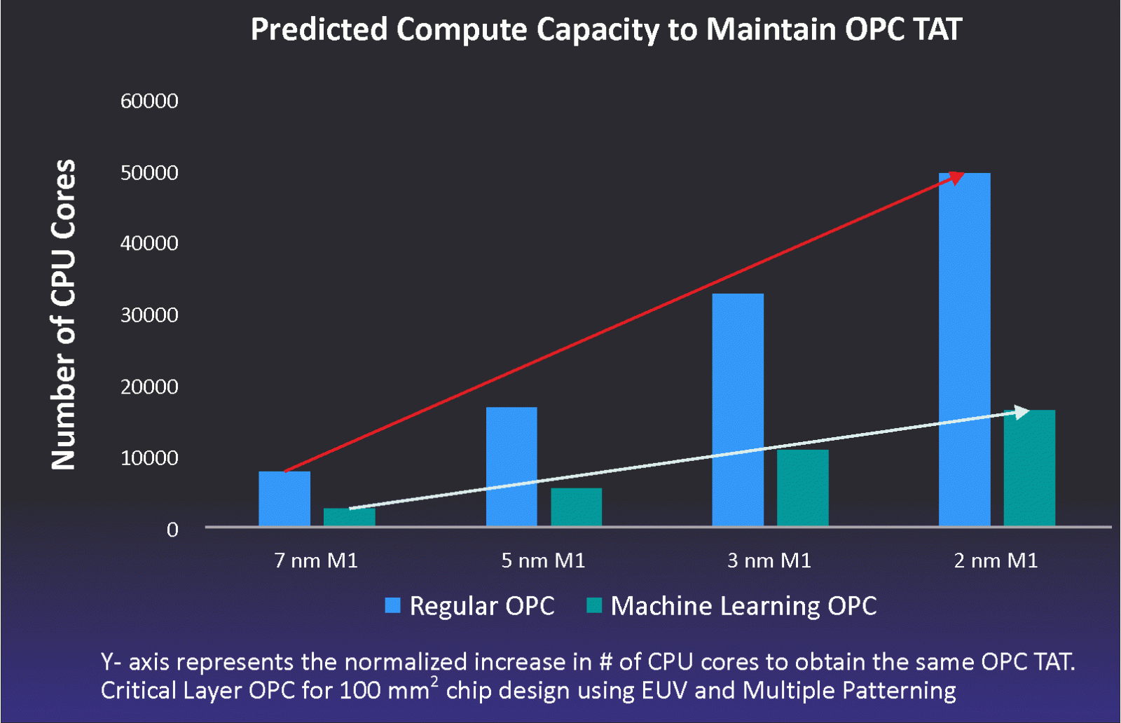
For example, for optical proximity correction, Calibre OPC operates on a physical design database. Each run of the chip produces billions of data points that are available for analysis. By putting ML technology into Calibre OPC, we can collect data around those chips and then use that to produce better results faster for designs.
At 7 nm for a critical layer, customers are using up to 8,000 CPUs running for 12 to 24 hours to perform a single run. By using machine learning, we have been able to drop that by a factor of three and constrain the increase in time that would be necessary to produce each of the advanced nodes coming in the future (see figure).
 |
||
| Figure 1. | Significant reduction in computational demand reduces significantly with machine-learning Calibre OPC in IC design tapeouts. |
|
This is just one example, but we’re seeing similar results with our other ML-enhanced tools. We currently have two dozen other projects in the works looking at new ways where AI/ML can leverage a seemingly abundant amount of data to deliver better results faster. You can certainly expect that in 2020, you’ll be using more ML-enhanced EDA tools to produce more innovations.