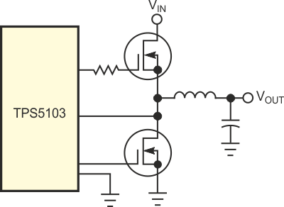
In a synchronous, buck switching power supply, the two FETs and the output inductor meet at the phase node (Figure 1). The phase node often connects directly to the control IC. The voltage on this node swings from the input voltage to some voltage lower than ground. If the voltage goes too far below ground, the ESD structures or other circuitry within the control IC can become forward-biased, causing currents to flow through the chip's substrate. These unwanted currents can cause erratic behavior and damage to the IC under certain circumstances. Although it is impossible to keep the phase node from going below ground, it is necessary to keep the voltage at the control IC from going so far negative that it adversely affects or damages the IC.
 |
||
| Figure 1. | This classic buck regulator suffers from excessive negative phase-node voltage. |
|
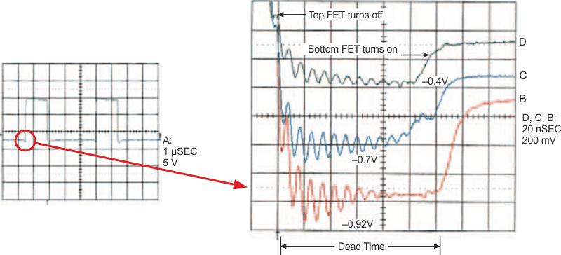
Trace A in Figure 2a shows the phase-node voltage waveform with VIN = 12 V, and VOUT = 3.5 V at 8 A. When the top FET is on, the output current flows through that FET and the inductor to the output. During this time, the phase-node voltage is equal to VIN. The bottom FET must remain off until after the top FET fully turns off. When the top FET turns off, the current then flows from ground, through the bottom FET, and through the output inductor. Dead time is the time lag between turning off the top FET and turning on the bottom FET. During the dead time, the current flows through the body diode of the bottom FET, and the phase-node voltage is approximately –1 V, depending on the current levels and the FET parameters. When the bottom FET turns on, the current flows through the FET structure rather than through the body diode. During this time, the voltage is a function of the output current and the resistance of the FET.
 |
||
| Figure 2. | Expanding the dead-time waveforms (a) leads to three scenarios (b): the unadorned buck regulator (Trace B), adding a Schottky diode (Trace C), and the simple solution in Figure 3 (Trace D). |
|
During the dead time, the negative voltage coupled with parasitic ringing can apply a negative voltage that exceeds the maximum voltage ratings of the control IC. Trace B in Figure 2b shows the phase node when the top FET turns off. The output current flows through the body diode of the bottom FET, and the voltage drop across the FET is –0.76 V. With the ringing in the circuit, the phase-node voltage can exceed –1 V, a voltage applied directly to the control IC. When the bottom FET turns on, the voltage drops to approximately –0.1 V (8 A × 0.013 Ω). Adding a Schottky diode in parallel with the bottom FET helps, but a Schottky diode is large and expensive and has little effect on the voltage. Trace C in Figure 2b shows the voltage that occurs with the addition of a large D-Pak MBRD835L Schottky diode. The diode reduces the voltage to –0.6 V. With ringing, the control IC sees –0.7 V.
 |
||
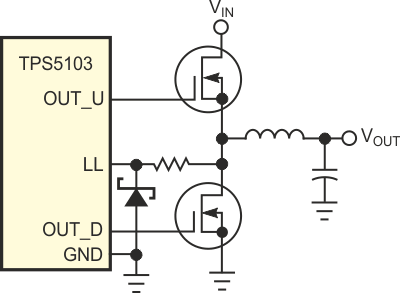
| Figure 3. | Moving one resistor and adding a small Schottky diode minimizes the phase-node voltage. |
|
The circuit in Figure 3 is small and inexpensive and significantly reduces the phase-node voltage at the control IC. The gate-drive resistor moves from the gate to the source of the top FET. Following the current from the IC as it charges and discharges the gate capacitance of the top FET shows that moving the resistor has no effect on the circuit operation. An SOT-23 or an SOD-123 Schottky diode with a current rating of 0.5 A connects to the control IC. As you can see in Trace D of Figure 2b, when the voltage across the FET's body diode goes to –1 V, the Schottky diode clamps the voltage on the IC to approximately –0.3 V. The full output current flows through the FET, and the gate-drive resistor limits the current through the Schottky diode. This solution is small and inexpensive and prevents erratic operation or damage to the power-supply control IC.