The Microchip PIC16F628A has always been my first choice for microcontroller-based projects. It is simple, inexpensive, and easily available. Due to its compact size (18 pins) it occupies lesser space on the circuit board, and meanwhile, it is powerful enough to serve most of a hobbyist’s needs. It is a very well accepted successor of the classic PIC16x84, and therefore, the tons of resources available for PIC16x84 on the internet and books can also be used for PIC16F628A. Last month, Microchip Technology Inc. announced the latest addition to its Enhanced Mid-Range core 8-bit PIC microcontroller (MCU) family by introducing PIC16F(LF)1847. When I went through its features I was tempted. The newly released PIC16F1847 seems to be the most powerful successor of the 18-pin PIC16F series of microcontrollers. It is pin-compatible with PIC16F628A but equipped with lot more peripherals and enhanced features. It has 14Kbytes of on-chip flash memory and 1KByte of data RAM. Now I never have to switch to a higher-end or bigger size PIC just because of the shortage of program memory or RAM. This would probably be the first 18-pin PIC device of the mid-range 8-bit family with so much of RAM and flash memory. Before this, Microchip also released PIC16F1827, similar to PIC16F1847 in peripherals and other features but with lesser program memory. I thought of doing some experiments with these two members of enhanced mid-range 8-bit PIC family and so decided to make my own development board for PIC16F1827/47. Making a development board is a one-time effort, and life becomes much easier after that.
Development board for PIC16F1827/47
Theory
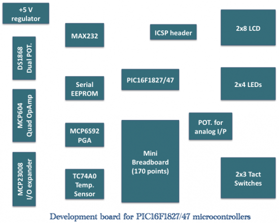
A development board is very helpful while exploring the different features of any microcontroller. It saves your time of wiring the circuit on a breadboard to do an experiment and later modify it for another experiment once you finished with the previous one, and so on. The development board allows you to perform any experiment or develop a project with minimum amount of effort and time. There is no standard circuit diagram for a microcontroller development board. It’s up to you what features you want on the board. Here’s what I decided to have on my board:
- An ICSP header to connect PIC16F1847 to PICkit3
- On-board voltage regulator (+5 V)
- A HD44780 based character LCD display
- 8 LEDs to read the status of output pins
- 6 Tact switches for providing inputs
- A potentiometer for providing analog input
- TTL to RS232 voltage level translation and vice-versa for serial interface
- An external serial EEPROM (24LC512)
- A GPIO expander (MCP23008)
- Quad OpAmp IC (MCP602) for signal conditioning
- Digital potentiometers (DS1868)
- Programmable gain amplifiers (MCP6S92)
- A temperature sensor (TC74A0)
- A mini breadboard
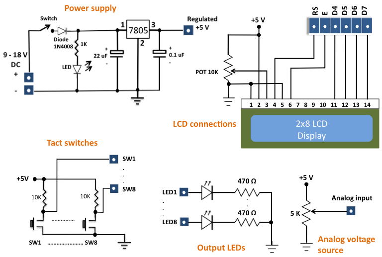
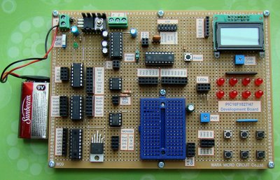
The layout of these components on the board is shown below. I soldered these components on a 18 cm × 12.8 cm experimenters circuit board. The PIC16F1827/47 is peripheral rich and each I/O pin serves multiple functions. Therefore, none of the I/O pins of PIC16F1827/47 are dedicatedly connected to any other peripheral components. Rather, individual pins are made easily accessible through double row female headers so that we can connect every peripheral device to whatever pins of PIC16F1847 we want to.
I printed labels on paper and stuck those on the board so that it would be easier to identify which pins go to what headers. The board can be powered from a 9V battery and the on-board regulator (LM7805) generates +5V power supply for the microcontroller and peripherals. The circuit diagram is pretty simple. The microcontroller and the peripherals’ power supply pins are connected to Vcc and Gnd, whereas the operational pins are connected to headers. There are some other pins besides the power supply, which are also needed to be connected to either Vcc or Gnd. For example, the external hardware address pins of I2C slave devices. The figure below shows the connection diagram of PIC16F1827/47 and header pins.
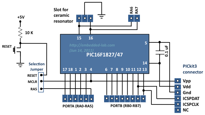
You can see there is a jumper selection for RA5/MCLR pin, which can be used as external reset or a general purpose input pin (RA5). The system clock for PIC16F1827/47 can be derived using an external ceramic resonator. There is a 3-pin slot for that. Taking the resonator out of the slot and using the internal clock source, the RA6 and RA7 pins can be used as general purpose input and output pins.
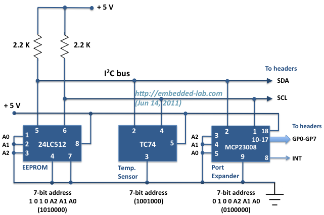
There are three I2C devices on the board: MCP23008 (8-bit port expander from Microchip), TC74 (temperature sensor from Microchip), and 24LC512 (EEPROM from Microchip). The external address pins of MCP23008 and 24LC512 are grounded. The TC74 temperature sensor does not have any external address pins. The figure below shows the connections for these three devices and their corresponding 7-bit slave addresses.
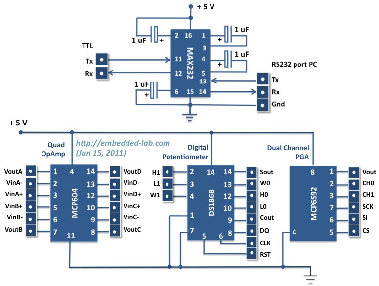
Similarly, the circuit diagram shown below describes the connections for UART interface, MCP604 (Quad OpAmp), DS1868 (digital potentiometer), and MCP6S92 (programmable gain amplifier). The translation between TTL and RS232 voltage levels is achieved using MAX232 chip that requires four external capacitors (each 1 uF) for its internal charge pumps. MCP604 is a quad OpAmp IC from Microchip that provides low bias current, high-speed operation, high open-loop gain and rail-to-rail output swing. DS1868 is a dual channel digital potentiometers with 256 wiper positions. The two potentiometers can be used independently or stacked for increased total resistance and number of taps. Communication takes place through a 3-wire serial port interface. The MCP6S92 is a 2-channel analog Programmable Gain Amplifier from Microchip. It can be configured for gains from 1 to 32 and the input multiplexer can select one of the two channels through a SPI port. It is optimized for high-speed, low offset voltage and single-supply operation with rail-to-rail input and output capability.
Next comes the circuit diagram for power supply, tact switches, LCD, and LEDs. For regulated +5V power supply, LM7805 IC is used. A general purpose diode is connected in series with the input of LM7805 for protecting against the wrong polarity of battery input. A 6-pin female header provides access to the LCD data and control pins. Tact switches are configured as active low, i.e, under normal conditions the tact switch output is high. A separate 5K potentiometer on the board will serve as a source of analog voltage.