Dave Salerno, Linear Technology
The proliferation of wireless sensors supporting the “Internet of Things” has increased the need for small, efficient power converters tailored to untethered low power devices. The new LTC3129 and LTC3129-1 are designed to satisfy this need. The LTC3129 and LTC3129-1 are monolithic buck-boost DC/DC converters with an input voltage range of 2.42 V to 15 V. The LTC3129 has an output voltage range of 1.4 V to 15.75 V, while the LTC3129-1 offers eight pin-selectable fixed output voltages between 1.8 V and 15 V. Both parts can supply a minimum output current of 200 mA in buck mode.
Low power sensors can rake advantage the LTC3129's and LTC3129-1's zero current when disabled (on both VIN and VOUT), and a quiescent current on VIN of just 1.3 µA when power saving Burst Mode® operation is selected, making them ideal for power and energy harvesting applications, where high efficiency at extremely light loads is crucial. Their buck-boost architecture makes them well suited to a wide variety of power sources.
Other key features of the LTC3129 and LTC3129-1 include a fixed 1.2 MHz operating frequency, current mode control, internal loop compensation, automatic Burst Mode operation or low noise PWM mode, an accurate RUN pin threshold to allow the UVLO threshold to be programmed, a power good output and an MPPC (maximum power point control) function for optimizing power transfer when operating from photovoltaic cells.
The compact 3 mm × 3 mm QFN package and the high level of integration ease the LTC3129/LTC3129-1's placement into space-constrained applications. Only a few external components and an inductor, which can be as small as 2 mm × 3 mm, are required to complete the power supply design. Internal loop compensation further simplifies the design process.
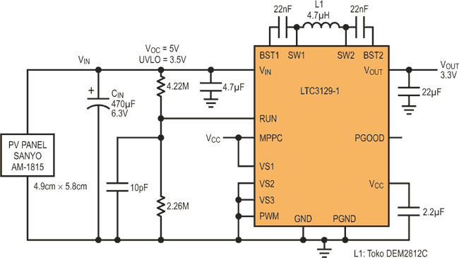
3.3V Converter Operates from Indoor Light Using a Small Solar Cell
The circuit in Figure 1 exploits the unique ability of the LTC3129 and LTC3129-1 to start up and operate from an input power source as weak as 7.5 microwatts – making them capable of operating from small (less than 1 in2), low cost solar cells with indoor light levels less than 200-lux. This enables such applications as indoor light powered wireless sensors, where the DC/DC converter must support an extremely low average power requirement, due to a low duty cycle of operation, from very low available power, while consuming as little power as possible.
 |
|
| Figure 1. | 3.3 V solar powered converter operates from indoor light. |
To make this low current start-up possible, the LTC3129 and LTC3129-1 draw a meager two microamps of current (less in shutdown) until three conditions are satisfied:
- The RUN pin must exceed 1.22 V (typical).
- The VIN pin must exceed 1.9 V (typical).
- VCC (which is internally generated from VIN but can also be supplied externally) must exceed 2.25 V (typical).
Until all three of these conditions are satisfied, the part remains in a "soft-shutdown" or standby state, drawing just 2 µA.
This allows a weak input source to charge the input storage capacitor until the voltage is high enough to satisfy all three previously mentioned conditions, at which point the LTC3129/LTC3129-1 begins switching, and VOUT rises to regulation, provided the input capacitor has sufficient stored energy. The input voltage at which the part exits UVLO can be set anywhere from 2.4 V to 15 V using the external resistive divider on the RUN pin. With a RUN pin current of less than 1 nA typical, high value resistors may be used to minimize current draw on VIN.
In the application example shown in Figure 1, the energy stored on CIN is used to bring VOUT into regulation once the converter starts. If the average power demand on VOUT is less than the power delivered by the solar cell, the LTC3129/LTC3129-1 remains in Burst Mode operation, and VOUT remains in regulation.
If the average output power demand exceeds the input power available, then VIN drops until UVLO is reached, at which point the converter reenters soft-shutdown. At this point, CIN begins recharging, allowing the cycle to repeat. In this hiccup mode of operation, VIN is positioned hysteretically about the UVLO point, with a VIN ripple of approximately 290 mV in this example. This ripple is set by the 100 mV hysteresis at the RUN pin, gained up by the UVLO divider ratio.
Note that by setting the converter's UVLO voltage to the MPP (maximum power point) voltage for the chosen solar cell (typically between 70% to 80% of the open-circuit voltage), the cell always operates near its maximum power transfer voltage (unless the average load requirement is less than the power output of the solar cell, in which case VIN climbs and remains above the UVLO voltage).
To further optimize efficiency and eliminate unnecessary loading of VOUT, the LTC3129/LTC3129-1 does not draw any current from VOUT during soft-start or at any time if Burst Mode operation is selected. This prevents the converter from discharging VOUT during soft-start, thereby preserving charge on the output capacitor. In fact, when the LTC3129 is sleeping, there is no current draw at all on VOUT. In the case of the LTC3129-1, the VOUT current draw is sub-microamp, due to the high resistance internal feedback divider.
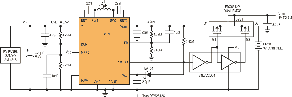
Adding a Battery Backup
In many solar powered applications, a backup battery provides power when solar power is insufficient. Figure 2 shows an application where a primary lithium coin cell and a few external components have been added to the converter from the previous example to provide backup power to the output in the event that the light source is unable to provide the necessary power to maintain VOUT. The LTC3129 is used in this case, allowing VOUT be programmed for 3.2 V to better match the voltage of the coin cell.
 |
|
| Figure 2. | Solar powered converter with coin cell backup. |
In this example, the battery is used on the output side of the converter, and the LTC3129 is set to regulate VOUT slightly above the battery voltage. This assures that there is no load on the battery whenever VOUT can be powered by the solar input. In the event that VOUT droops due to insufficient light to power the load, the PGOOD output from the LTC3129 goes low, switching the load from the converter output to the battery, thus holding VOUT at the battery voltage. During this time, the converter's input and output capacitors are able to recharge (if some light is available), enabling the load to be periodically switched from the battery back to the converter by the PGOOD signal. In this manner the load is powered by the solar input as much as possible, and the battery is only used in a time-shared manner, extending its life.
The diode connected from PGOOD to VCC is used to hold PGOOD low during start-up, before VCC (and therefore PGOOD) is valid.
Choosing Where to Put the Backup Battery
In the previous example, the backup battery was placed on the output. For light load applications, this has the advantage of not exposing the battery – which may be a low capacity battery with high internal resistance – to relatively high converter start-up input current bursts, causing significant battery droop and lossy internal power dissipation, in turn reducing battery life.
The disadvantages of putting the backup battery on the output of the converter are that the battery voltage must be well matched to the desired output voltage, and it must have a relatively flat discharge curve so as to maintain reasonable regulation of VOUT. The 3 V lithium cell satisfies both of these requirements.
Putting the backup battery on the input side of the converter allows its voltage to be different from the desired output voltage, but it must be able to withstand the higher currents that the converter draws during start-up or load transients. If used on the input side, a lithium-thionyl chloride battery is generally a better choice for long life applications. It can be diode-OR'd with the solar cell or switched in and out with MOSFET switches, in a similar manner to Figure 2.
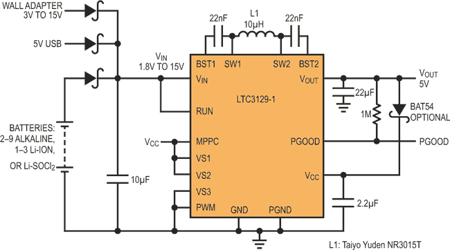
5 V Converter Operates Seamlessly from a Variety of Input Sources
The ability of the LTC3129-1 to operate at high efficiency over a wide range of loads and input voltages with a minimal number of external components is illustrated in Figure 3. In this example, the output, which has been programmed for 5 V using the VS1-VS3 pins, can be powered from a 5 V USB input, a variety of battery options or a 3 V to 15 V wall adapter. The flexibility of running seamlessly from a wide variety of power sources is an asset in critical field applications, such as military radios.
 |
|
| Figure 3. | Multi-input 5 V converter. |
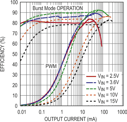
The LTC3129-1's low IQ of just 1.3 µA in sleep mode, combined with a high resistance internal feedback divider, enables it to maintain high efficiency over a wide range of loads, as shown in Figure 4. At a load current of just 100 µA, the efficiency is ~80% over nearly the entire VIN range. This is an important feature for extending battery life in applications that spend a large percentage of the time in a low power state.
 |
|
| Figure 4. | Efficiency vs VIN and load of the 5 V converter in Figure 3. |
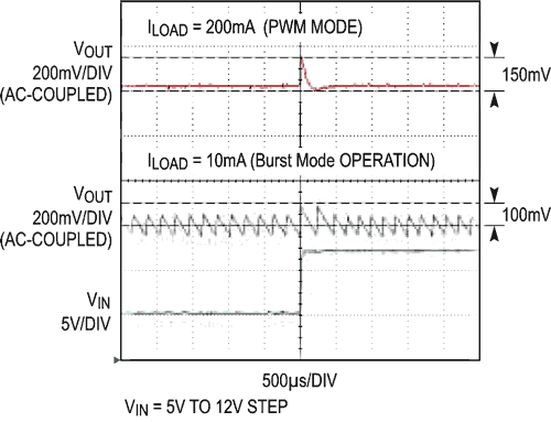
The line step response (VIN is stepped from 5 V to 12 V) is shown in Figure 5, with VOUT measured under both heavy and light load conditions. At a load of 200 mA, the part is operating in PWM mode, and VOUT overshoot is only 150 mV (3%). At a load of 10 mA, the part is in Burst Mode operation, with a burst ripple of 100 mVPK-PK (2%), and less than 100 mV of VOUT overshoot due to the line step.
 |
|
| Figure 5. | Line transient response of the 5 V converter in Figure 3. |
The VCC pin is the output of an internal LDO that generates a nominal 3.9 V from VIN to power the IC. The LDO is designed so that it can be externally back-driven up to 5 V. In this example, an optional bootstrap diode is shown from VOUT to VCC.
The addition of this external bootstrap diode has two advantages. First, it improves efficiency at low VIN and high load current by providing a higher gate drive voltage to the internal switches, lowering their RDS(ON). Also, at high VIN and light load, it improves efficiency by reducing the power lost in the internal LDO used to generate VCC. (Note that the VCC pin must not be raised above 6 V, so it cannot be diode-connected to higher output voltages.)
The second advantage of adding a bootstrap diode is that it allows operation from a lower VIN. After start-up, if VCC is held above its minimum value of 2.2 V (by the output voltage in this case), then the converter can operate at a lower input voltage, down to 1.75 V, where the fixed internal VIN UVLO threshold is reached. This capability extends the usable voltage range enough to make it possible to run from two depleted alkaline batteries. Note that if the battery voltage is below 2.4 V and the converter is shut down (or VOUT is shorted), the IC is not be able to restart.
Outdoor Solar Converter/Charger with MPPC
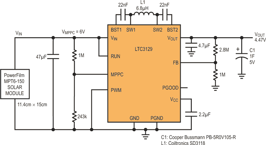
The LTC3129 and LTC3129-1 include a maximum power point control (MPPC) feature that allows the converter to servo VIN to a minimum voltage under load, as set by the user. Regulating VIN maintains optimal power transfer in applications using higher current solar cells or other sources with high internal resistance. This feature prevents the converter from crashing the input voltage when operating from a current-limited source.
The MPPC control loop operates by reducing the average inductor current commanded by the converter, thus maintaining the minimum programmed VIN voltage under load. This voltage is set using an external resistor divider connected to VIN and the MPPC pin, as shown in the supercapacitor charging example of Figure 6. The MPPC control loop is designed to be stable with a minimum input capacitance of 22 µF.
 |
|
| Figure 6. | Outdoor solar powered supercapacitor charger with maximum power point control. |
Note that reducing the inductor current under MPPC would cause the output voltage to droop if it were driving a conventional load. Therefore, most applications employing MPPC involve charging a large storage capacitor (or trickle charging a battery) from a solar cell. The MPPC feature assures that the capacitor or battery is charged at the highest current possible, while operating the solar cell at its maximum power point voltage.
It is important to note that when the LTC3129/LTC3129-1 is in MPPC control, Burst Mode operation is inhibited, and the VIN quiescent current is several milliamps, since the IC is switching continuously at 1.2 MHz. Therefore, MPPC is not appropriate for use with sources that cannot supply a minimum of about 10 mA. For applications requiring an MPPC-like function with very weak input sources, the accurate RUN pin should be used to program a UVLO threshold, as described in the example of Figure 1.
Intrinsic Safety Using MPPC
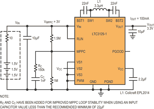
The MPPC feature can be used in other applications, including those designed for intrinsic safety, where the input source has a series current limiting resistor between it and the DC/DC converter. In this case, the MPPC loop prevents the LTC3129/LTC3129-1 from drawing too much current, especially during startup when the output capacitor is being charged, and crashing the input voltage. An example of this is shown in Figure 7, where the input voltage is maintained at a minimum of 3 V, as set by the MPPC divider.
 |
|
| Figure 7. | 3.3 V converter using MPPC for intrinsic safety application. |
In this case, because the input capacitor value is limited to just 10 µF for safety (less than the recommended minimum value of 22 µF when using MPPC), an additional RC compensation network is added to the MPPC pin for improved phase margin of the MPPC loop.
Input Current Limit Using MPPC
Note that the MPPC feature can be used to set the maximum input current to a given value. By choosing a series input resistor value and setting the MPPC voltage to a value below a fixed input source voltage, the maximum input current is limited to:
![]()
Conclusion
The LTC3129 and LTC3129-1 monolithic buck-boost DC/DC converters offer exceptional low power performance and power source flexibility demanded by real-world wireless sensor and portable electronic instruments. The ultralow 1.3 µA quiescent current and high conversion efficiency can extend battery lifetime indefinitely if used in concert with energy harvesting.
A choice of maximum power point control schemes allows optimization of power performance over a wide range of power sources. The expanding reach of wireless monitoring applications demands easy to use, efficient and flexible DC/DC power converter solutions. The LTC3129 and LTC3129-1 are ready to meet this challenge.