Requiring only a handful of inexpensive components, the circuit breaker in Figure 1 responds to both overcurrent- and overvoltage-fault conditions. At the heart of the circuit, D2, an adjustable, precision, shunt-voltage regulator, provides a voltage reference, comparator, and open-collector output, all integrated into a three-pin package.
 |
|
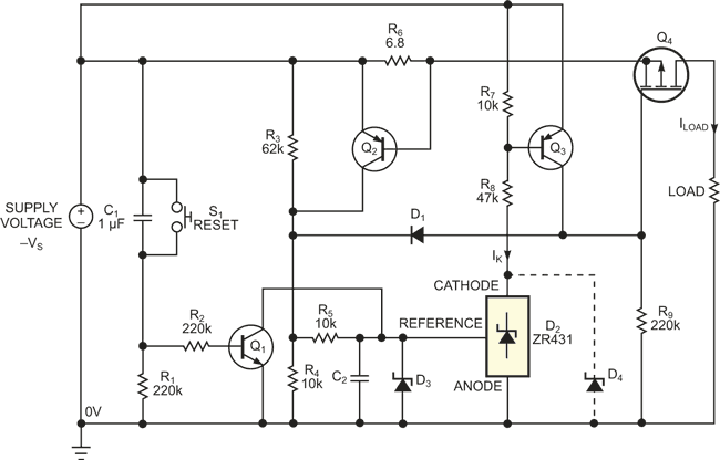
| Figure 1. | This circuit breaker provides both overvoltage and overcurrent protection. Other than the current flowing in R3, R4, and D2’s cathode, the circuit draws no current from the supply in its normal untripped state. |
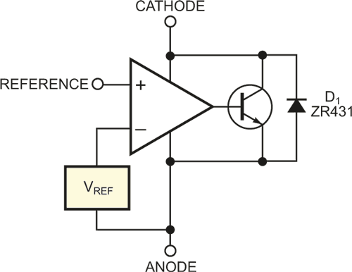
Figure 2 shows a simplified view of the ZR431, D1. The voltage appearing at the reference input is compared with the internal voltage reference, VREF, nominally 2.5 V. In the off state, when the reference voltage is 0 V, the output transistor is off, and the cathode current is less than 0.1 µA. As the reference voltage approaches VREF, the cathode current increases slightly; when the reference voltage exceeds the 2.5 V threshold, the device fully switches on, and the cathode voltage falls to approximately 2 V. In this condition, the impedance between the cathode and the supply voltage determines the cathode current; the cathode current can range from 50 µA to 100 mA.
 |
|
| Figure 2. | In this simplified view of the ZR431, the voltage at its reference input is compared with the internal voltage reference, which is nominally 2.5 V. |
Under normal operating conditions, D2’s output transistor is off, and the gate of P-channel MOSFET Q4 goes through R9, such that the MOSFET is fully enhanced, allowing the load current, ILOAD, to flow from the supply voltage, –VS, through R6 into the load. Q2 and current-sense resistor R6 monitor the magnitude of ILOAD, where Q2’s base-emitter voltage, VBE, is ILOAD×R6. For normal values of ILOAD, VBE is less than the 0.6 V necessary to bias Q2 on, such that the transistor has no effect on the voltage at the junction of R3 and R4. Because the input current at D2’s reference input is less than 1 µA, negligible voltage drops across R5, and the reference voltage is effectively equal to the voltage on R4.
In the event of an overload when ILOAD exceeds its maximum permissible value, the increase in voltage across R6 results in sufficient base-emitter voltage to turn on Q2. The voltage on R4 and, hence, the reference voltage now pull up toward VS, causing D2’s cathode voltage to fall to approximately 2 V. D2’s output transistor now sinks current through R7 and R8, thus biasing Q3 on. Q4’s gate voltage now effectively clamps to the supply voltage through Q3, and the MOSFET turns off. At the same instant, Q3 sources current into R4 through D1, thereby pulling the voltage on R4 to a diode drop below the supply voltage. Consequently, no load current flows through R6 because Q2, whose base-emitter voltage is now 0 V, has turned off. As a result, no load current flows through R6, D2’s output transistor latches on, and the circuit remains in its tripped state in which the load current is 0 A. When choosing a value for R6, ensure that Q2’s base-emitter voltage is less than approximately 0.5 V at the maximum permissible value of the load current.
As well as responding to overcurrent conditions, the circuit breaker also reacts to an abnormally large value of the supply voltage. When the load current lies within its normal range and Q2 is off, the magnitude of the supply voltage and the values of R3 and R4, which form a potential divider across the supply rails, determine the voltage at the reference input. In the event of an overvoltage at the supply voltage, the voltage on R4 exceeds the 2.5 V reference level, and D2’s output transistor turns on. Once again, Q3 turns on, MOSFET Q4 switches off, and the load becomes effectively isolated from the dangerous transient.
The circuit now remains in its tripped state until reset. Under these conditions, Q3 clamps Q4’s gate-source voltage to roughly 0 V, thereby protecting the MOSFET itself from excessive gate-source voltages. Ignoring the negligibly small voltage across R5, you can see that the reference voltage is
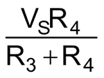
in volts. Because D2’s output turns on when the reference voltage exceeds 2.5 V, you can rearrange the equation as
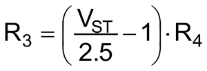
in ohms, where VST is the required supply-voltage trip level. For example, if R4 has a value of 10 kΩ, a trip voltage of 18 V would require R3 to have a value of 62 kΩ. When choosing values for R3 and R4 to set the desired trip voltage, ensure that they are large enough that the potential divider will not excessively load the supply. Similarly, avoid values that could result in errors due to the reference-input current.
When you first apply power to the circuit, you’ll find that capacitive, bulb-filament, motor, and similar loads having large inrush current can trip the circuit breaker, even though their normal, steady-state operating current is below the trip level that R6 sets. One way to eliminate this problem is to add capacitor C2, which slows the rate of change of the voltage at the reference input. However, although simple, this approach has a serious disadvantage in that it slows the circuit’s response time to a genuine overcurrent-fault condition.
Components C1, R1, R2, and Q1 provide an alternative solution. On power-up, C1 initially discharges, causing Q1 to turn on, thereby clamping the reference input to 0 V and preventing the inrush current from tripping the circuit. C1 then charges through R1 and R2 until Q1 eventually turns off, releasing the clamp at the reference input and allowing the circuit to respond rapidly to overcurrent transients. With the values of C1, R1, and R2, the circuit allows approximately 400 msec for the inrush current to subside. Selecting other values allows the circuit to accommodate any duration of inrush current you apply to a load. Once you trip the circuit breaker, you can reset it either by cycling the power or by pressing S1, the reset switch, which connects across C1. If your application requires no inrush protection, simply omit C1, R1, R2, and Q1 and connect S1 between the reference input and 0 V.
When choosing components, make sure that all parts are properly rated for the voltage and current levels they will encounter. The bipolar transistors have no special requirements, although these transistors, especially Q2 and Q3, should have high current gain, Q4 should have low on-resistance, and Q4’s maximum drain-to-source and gate-to-source voltages must be commensurate with the maximum value of supply voltage. You can use almost any small-signal diode for D1. As a precaution, it may be necessary to fit zener diodes D3 and D4 to protect D2 if extremely large transient voltages are likely.
Although this circuit uses the 431 device, which is widely available from different manufacturers, for D2, not all of these parts behave in exactly the same way. For example, tests on a Texas Instruments TL431CLP and a Zetex ZR431CL reveal that the cathode current is 0 A for both devices when the reference voltage is 0 V. However, gradually increasing the reference voltage from 2.2 to 2.45 V produces a change in cathode current ranging from 220 to 380 µA for the TL431CLP and 23 to 28 µA for the ZR431CL – roughly a factor of 10 difference between the two devices. You must take this difference in the magnitude of the cathode current into account when selecting values for R7 and R8.
The type of device you use for D2 and the values you select for R7 and R8 can also have an effect on response time. A test circuit with a TL431CLP, in which R7 is 1 kΩ and R8 is 4.7 kΩ, responds within 550 nsec to an overcurrent transient. Replacing the TL431CLP with a ZR431CL results in a response time of approximately 1 µsec. Increasing R7 and R8 by an order of magnitude to 10 and 47 kΩ, respectively, produces a response time of 2.8 µsec. Note that the relatively large cathode current of the TL431CLP requires correspondingly small values of R7 and R8.
To set the overvoltage-trip level at 18 V, R3 and R4 must have values of 62 and 10 kΩ, respectively. The test circuit then produces the following results: Using a TL431CLP for D2, the circuit trips at 17.94 V, and, using a ZR431CL for D2, the trip level is 18.01 V. Depending on Q2’s base-emitter voltage, the overcurrent-detection mechanism is less precise than the overvoltage function. However, the overcurrent-detection accuracy greatly improves by replacing R6 and Q2 with a high-side current-sense amplifier that generates a ground-referred current proportional to load current. These devices are available from Linear Technology, Maxim, Texas Instruments, Zetex, and others.
The circuit breaker should prove useful in applications such as automotive systems that require overcurrent detection to protect against faulty loads and that also need overvoltage protection to shield sensitive circuitry from high-energy-load-dump transients. Other than the small current flowing in R3 and R4 and the current in D2’s cathode, the circuit draws no current from the supply in its normal, untripped state.