This Design Idea offers a new instrumentation-amplifier topology that improves ac CMR (common-mode rejection). Because it uses discrete amplifiers, you can customize it for the lowest power, price, noise, and supply voltage, depending on your application’s requirements. Previously, instrumentation amps using discrete components had poor CMR. System designers still build their own using discrete designs because standard integrated instrumentation amps don’t meet their design requirements, have undesired package options, or are too expensive. You can build discrete instrumentation amps with two or three op amps and a few resistors (Figure 1). Most monolithic instrumentation amps, however, use the three-op-amp configuration. This approach provides the best ac and dc CMR. A big challenge when building discrete instrumentation amps is to achieve CMR on par with that of monolithic instrumentation amps.
|
||||||
| Figure 1. | You can use conventional two-op-amp (a) and three-op-amp (b) configurations to build an instrumentation amplifier. | |||||
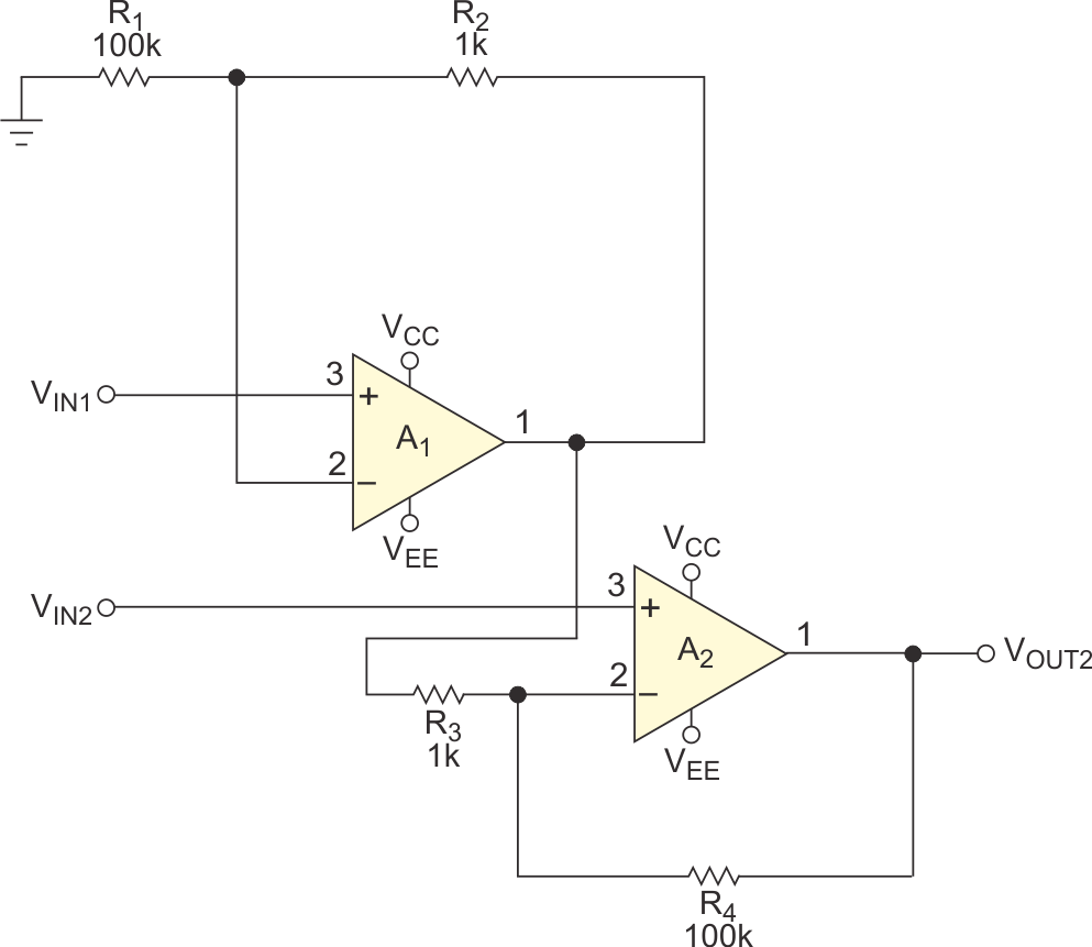
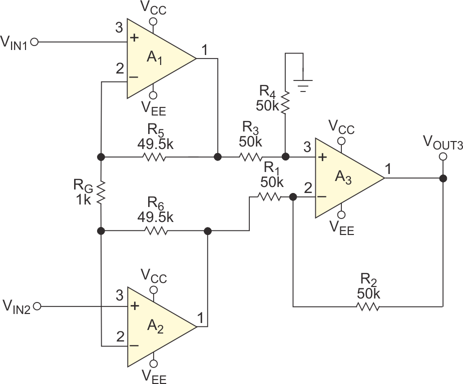
The poor CMR of the three-op-amp topology (Figure 1b) is due to resistor mismatching. Any common-mode signal at VIN1 and VIN2 appears at the outputs of A1 and A2. The difference amplifier, comprising R1, R2, R3, R4, and A3, should reject this common-mode voltage. To achieve high CMR, this difference amplifier requires matched resistors and the A3 op amp, which specifies high CMR. With 0.1%-resistor matching, the best possible CMR at dc is 54 dB. This CMR further degrades over frequency, depending on the op amp you select.
The poor CMR in two-op-amp instrumentation amps (Figure 1a) is due to the unequal phase shift that occurs at the two inputs of A2. Signal VIN1 must travel through amplifier A1 before amplifier A2 subtracts it from VIN2. Thus, the voltage at the output of A1 becomes delayed with respect to VIN1. Amplifier A1 introduces the delay that causes its output to lag behind the directly applied input voltage at VIN2. This phase difference results in an instantaneous difference in A1’s output and VIN2, even if the amplitudes of both voltages are equal. This difference causes a frequency-dependent common-mode error voltage at VOUT. Further, this ac common-mode error increases with common-mode frequency because the phase shift through A1 increases with frequency due to the single-pole roll-off frequency response.
Instrumentation-amplifier-design guidelines give the error relationship, according to the following equation:
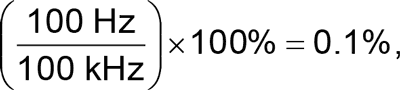
when you design an instrument amplifier for a closed-loop bandwidth of 100 kHz by using micropower op amps with a unity-gain bandwidth of 500 kHz configured for a gain of five (Reference 1). A common-mode error of 0.1% is equivalent to a 60-dB CMRR (common-mode-rejection ratio). Even if you trim this circuit to achieve 100-dB CMRR at dc, this performance would hold only for frequencies less than 1 Hz. At 100 Hz, the CMRR could not be better than 60 dB.
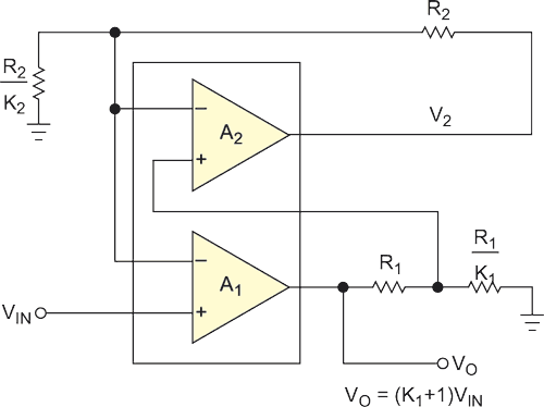
You can overcome the shortcomings of the two-op-amp circuit if you compensate for the phase delay of A1 using active-feedback compensation. You can reduce phase error to virtually zero at low frequencies with a dual matched op amp (Reference 2). This approach adds an equal but opposite phase shift in the amplifier’s feedback loop. Because the circuit depends on amplifier matching, you must use a dual- or quad-op-amp part.
 |
||
| Figure 2. | Using A2 in an active-feedback network greatly improves A1’s effective bandwidth. The op amps must match, so you should use a dual-amplifier package for this circuit. |
|
The active feedback requires an extra op amp and two external resistors to achieve phase-error cancellation (Figure 2). In the circuit, amplifier A1 provides forward gain of the composite amplifier. K1 determines the closed-loop gain
(AV = 1 + K1),
where AV is voltage gain and K1 is a constant. Amplifier A2 provides feedback to amplifier A1. K2 determines the amount of phase-error compensation and has no effect on the forward gain of the composite amplifier. Optimum error cancellation occurs when K1 is equal to K2. The error terms are functions of complex frequency response, according to the following equations:
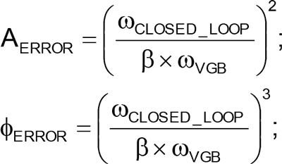
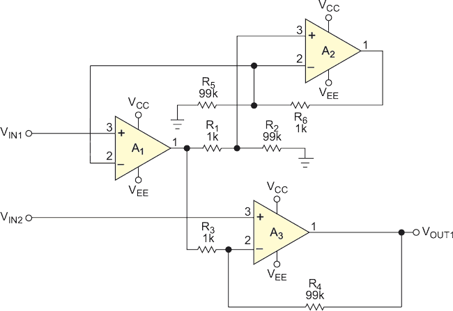
Figure 3 shows the new configuration, which applies an active feedback network to a two-op-amp configuration. You correct the phase delay through A1 using the active-feedback circuitry comprising A2 and four resistors. The classic two- and three-amplifier instrumentation amplifiers and this proposed three-amplifier topology using active feedback have similar dc CMRRs. However, the circuits’ ac CMRs differ. This difference in performance arises when you apply and sweep a large ac common-mode voltage at the input. These test specs are for a circuit using Analog Devices’ AD8603 op amps. The supply voltage is ±2.5 V, the common-mode voltage is 0.001 mV, and the gain is 100. You take error measurements with a 500-Hz input signal.
 |
||
| Figure 3. | The three-op-amp instrumentation amplifier employs a two-amplifier topology; a third amplifier provides active-feedback phase compensation. |
|
You then change the operating conditions to a common-mode voltage of 2.001 V and a gain of 100. The circuit in Figure 3 provides great improvement over the circuit in Figure 1a. The circuit has less sensitivity to resistor mismatch than the circuit in Figure 1b with perfectly matched resistors.