Greg Davis
Electronic Design
Whether it’s a vision-correction medical instrument or factory press, INAs offer an excellent way to amplify microvolt-level sensor signals while simultaneously rejecting high common-mode signals.
In the past, the term instrumentation amplifier (INA) was often misused, referring to the application rather than the device’s architecture. INAs are related to op amps, in that they’re based on the same architecture, but an INA is a specialized version of an op amp. INAs are specifically designed and used for their high differential gain to amplify microvolt-level sensor signals while simultaneously rejecting high-common-mode signals that can be several volts. This is important since some sensors produce a relatively small change in voltage or current, and this small change must be accurately captured.
Let’s consider a few applications that benefit from INAs. For example, a medical instrument that uses sensors to align laser stepper motors for vision-correction eye surgery. High accuracy is crucial, and other equipment in the operating room can’t be allowed to compromise the sensor signals and cause unexpected results.
Another example is a factory press. These machines apply thousands of pounds of force to bend metal into shapes. Using sensors, these machines are designed to stop if it detects a human hand. In this example, it’s critical that electrical noise from other factory equipment doesn’t cause interference that could lead to a malfunction.
In both cases above, the first step in the journey of the sensor signal is through an instrumentation amplifier. The tiny sensor signals must be accurately amplified in all environments. Instrumentation amplifiers are specially designed to do exactly that – to accurately amplify small signals resulting in high gain accuracy in an electrically noisy environment.
Other considerations further enhance the performance of an INA. Low power consumption is important to extend battery life. A low operating voltage allows the battery to be used over more of its depletion curve, extending battery life. A wide input voltage range allows compatibility with more sensors. And impedance matching at the input contributes to the seamless interface to sensors.
How INA Designs Have Evolved
With an endless number of consumer, medical, and industrial applications, designs have evolved over the years to take advantage of the performance benefits offered by INAs. Let’s look at the evolution of INA designs, from the original approaches to the instrumentation amplifiers available today. By reviewing these architectures and their associated strengths and limitations, this article shows the performance improvements seen in present-day instrumentation amplifiers along with real-life applications.
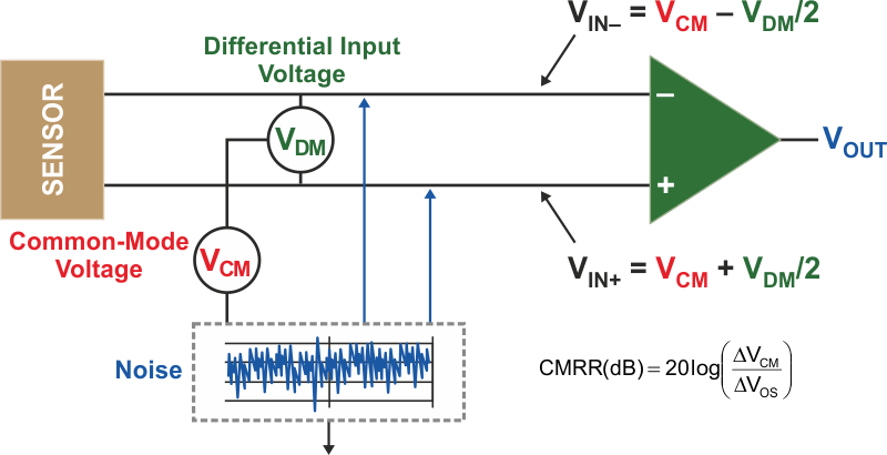
Before delving into the different approaches, let’s first look at what we’re trying to accomplish, using the diagram in Figure 1.
 |
||
| Figure 1. | Block diagram of sensor interface to INA. | |
The sensor outputs are connected to the INA inputs that amplify the differential voltage. Noise comes from many sources, both radiated and conducted. Typical noise may derive from switching power supplies, motors, and wireless devices. Such noise is reduced by shielding and good PCB layout practices; however, some noise will get through.
Fortunately, most of that noise shows up as an in-phase, common-mode voltage (VCM) superimposed on the differential input sensor voltage (VDM), and a properly designed instrumentation with good common-mode rejection ratio (CMRR) will greatly reduce this voltage to maintain gain accuracy. A minimum CMRR is typically specified at dc, while the ac CMRR performance is documented in performance curves.
The Discrete Difference Amplifier
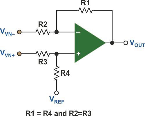
If you want to amplify the voltage difference across the sensor output, a simple difference amplifier works, but it has many downsides. In the simple implementation shown in Figure 2, VIN+ is biased to VREF (typically half the supply voltage) for single-supply applications.
 |
||
| Figure 2. | Discrete difference amplifier. | |
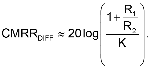
Designed to amplify differential voltages, the operational amplifier itself provides good CMRR, but this is overwhelmed by the circuit surrounding it. Any mismatch in the external resistors (including mismatch contributed by any divider network connected to VREF) limits the ability of the op amp to reject common-mode signals, resulting in reduced CMRR. Resistor tolerances are simply not tight enough to maintain a good CMRR that would be expected from an INA. We can see how much the resistor mismatch affects CMRR using the equations below.
The equation below uses a difference amplifier with G = 1 V/V, and TR is the resistor tolerance:
- If TR = 1%, worst-case dc CMRRDIFF will be 34 dB
- If TR = 0.1%, worst-case dc CMRRDIFF will be 54 dB
where ‘K’ is the net matching tolerance of R1/R2 to R3/R4, and K can be as high as 4TR (worst case):
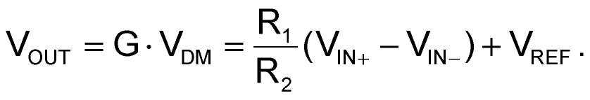
The amplifier amplifies the differential voltage at the input, and the gain of the amplifier is:
The problem is that the differential voltage (VIN- and VIN+) includes superimposed noise, and any common-mode voltage that’s not rejected (due to poor CMRR) will be amplified, resulting in an output being corrupted by noise.
This simple approach also has other drawbacks. Typically the input impedance of an operational amplifier is high (MΩ to GΩ range). However, because of the feedback path and reference, the impedance is both reduced and imbalanced, thus loading the sensor and adding to inaccuracies. While this circuit will amplify a small signal sensor, the poor gain accuracy in the presence of noise would not be useful for instrumentation purposes.
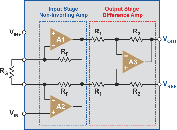
The Three Op-Amp IC Approach
This is a common INA packaged in a single integrated circuit (IC) (Fig. 3). The circuit is divided into two stages: The input stage has two inverting buffer amplifiers, and the output stage is a traditional difference amplifier. The internal resistors used throughout this design are matched to a very close tolerance only possible with trimmed resistor semiconductor designs, resulting in a much higher CMRR.
 |
||
| Figure 3. | Three-operational-amplifier IC approach. | |
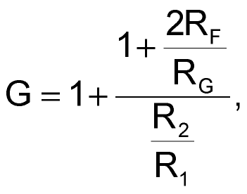
The input-stage amplifiers also provide high impedance, which minimizes loading of the sensors. The gain-setting resistor (RG) allows the designer to select any gain within the operating region of the device (typically 1 V/V to 1000 V/V).
The output stage is a traditional difference amplifier. The ratio of internal resistors, R2/R1, sets the gain of the internal difference amplifier, which is typically G = 1 V/V for most instrumentation amplifiers (the overall gain is driven by the amplifier in the first stage). The balanced signal paths from the input to the output yield excellent CMRR.
The design is simple to implement, has a small footprint, and fewer components, leading to lower system costs. The design is also compatible with single-source supplies using the VREF pin. However, even with this design, there are limitations to consider.
Three op-amp INAs achieve high CMRR at dc by matching the on-chip resistors of the difference amplifier, but the feedback architecture can substantially degrade the ac CMRR. In addition, parasitic capacitances can’t be completely matched, causing mismatches and reduced CMRR over frequency. The common-mode voltage input range is limited so that internal nodes don’t saturate. The VREF pin requires a buffer amplifier for optimal performance. Lastly, the temperature coefficient of the external and internal gain resistors aren’t matched, which contributes to a decline in CMRR.
Mathematically, the gain accuracy depends on resistor matching:

where:
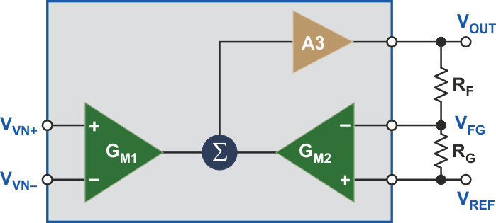
The Indirect Current Feedback Approach
The indirect current feedback (ICF) INA uses a novel voltage-to-current conversion approach (Fig. 4). It’s comprised of two matched transconductance amplifiers, GM1 and GM2, and a high-gain transimpedance amplifier (A3). The design doesn’t rely on balanced resistors, so internally trimmed resistors aren’t required, thereby reducing manufacturing cost. Another advantage is that the external resistors needn’t match any on-chip resistors. Only the RF and RG external resistors temperature coefficients need to match as closely as possible for minimal gain drift.
 |
||
| Figure 4. | Indirect current feedback approach. | |
The dc CMRR is high since amplifier GM1 rejects common-mode signals. And ac CMRR doesn’t decrease significantly with increased frequency. It was mentioned that the three-op-amp approach input range is limited to prevent internal node saturation. With an ICF, the output voltage swing isn’t coupled to the input common-mode voltage, resulting in an expanded range of operation not possible with the three-op-amp architecture.
The second stage (GM2 and A3) differentially amplifies the signal and further rejects common-mode noise on VFG and VREF. Single-supply operation can still be used by applying a bias to VREF.
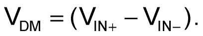
The ICF INA gain is:

where: VDM is the differential-mode voltage:
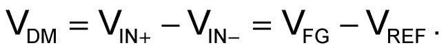
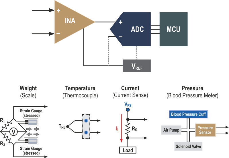
Figure 5 shows a few typical applications for an INA. A variety of sensors are shown that are accurately amplified by an INA feeding a converter and microcontroller.
 |
||
| Figure 5. | Shown are examples of a typical circuit using an INA with a sensor. | |
Conclusion
The need to amplify small signals in the presence of noise has gone through an evolution over the years. The simplest approach, the discrete operational amplifier, isn’t suitable as an INA. The integrated three-op-amp approach has significant advantages, including high dc CMRR, and balanced and high input impedances with one gain resistor. However, there are common-mode voltage limitations and it’s difficult to match internal versus external resistor temperature coefficients, resulting in gain drift. The impedance at the VREF pin can also negatively impact CMRR unless a buffer is used.
The ICF approach also has a high CMRR (even at higher frequencies), a wider common-mode voltage range and no on-chip trimmed resistors resulting in lower cost and low temperature-coefficient gain drift.