Marián Štofka
EDN
Many applications require a sampling circuit whose output is inverted with regard to the respective sample of an input signal. A simple approach is a cascade of a common noninverting sample-and-hold amplifier and an inverting amplifier. A classic inverting amplifier is an op amp with voltage feedback from two resistors. The values of these resistors, which are usually equal, should be high enough to decrease the total power loss of
which is proportional to the square of the output voltage. The values of these resistors should be as low as possible to preserve the bandwidth of the op amp.
Any parasitic capacitance (C2 in the following equation) parallel to feedback resistor R2 forms a pole in the transfer function of the inverter. This pole results in an additional breakdown of the gain-frequency characteristic of the inverting amplifier, with the value of breakdown frequency of
To retain the widest possible bandwidth, f2 > fT, where fT is the transition frequency of the op amp – in other words, the frequency at which the open-loop gain of the op amp drops to unity.
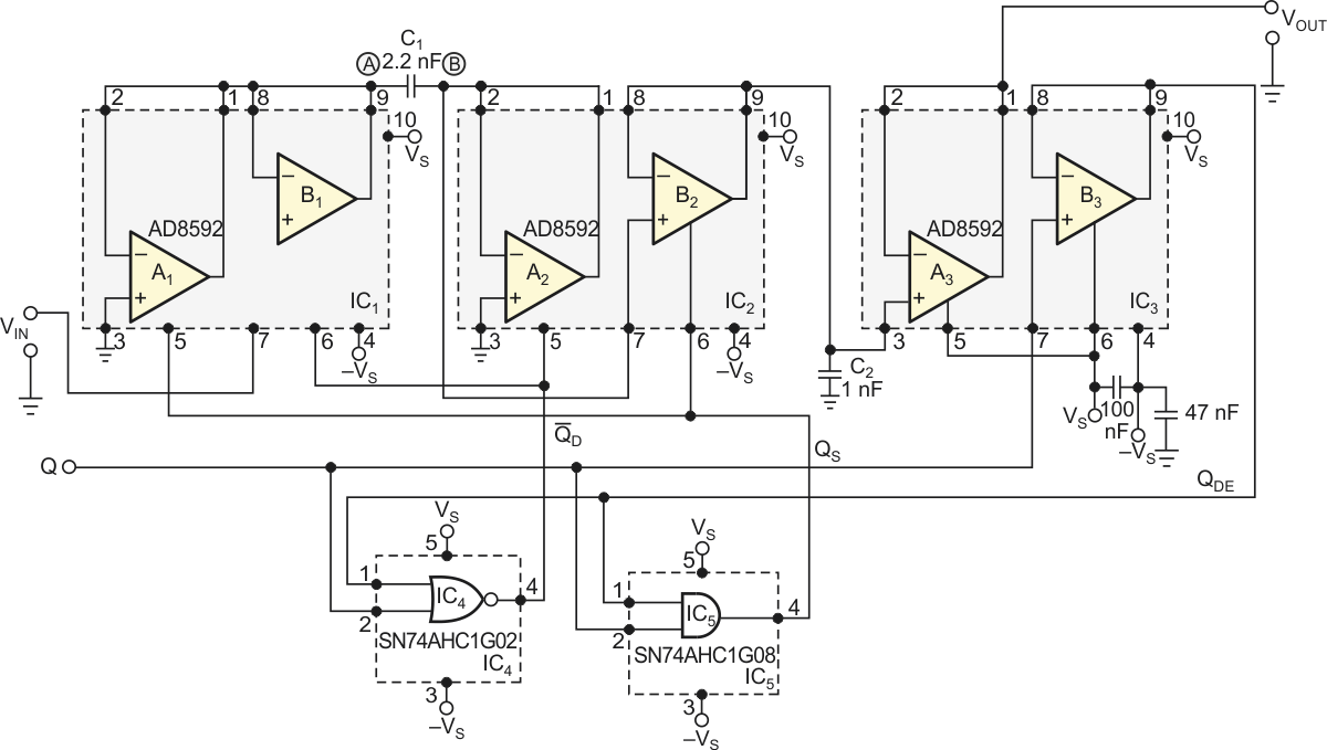
The Analog Devices’ AD8592 dual op amps, which have a high-quality shutdown function, allow you to use a different approach. The inverting sample-and-hold circuit in Figure 1 uses no external resistors. Thus, no power dissipates at external passive devices in the hold state of the circuit. All op amps act as voltage followers. In the hold state, followers B1 and A2 are enabled; thus, the B lead of the C1 capacitor, Pin 1 of IC2, is grounded through the output of A2, and the input voltage, VIN, gets followed at the A lead of the C1, Pin 9 of IC1. Upon the sampling command, Q is high, and, at this time, the A lead of C1 gets grounded through the output of the A1 follower. This scenario causes a negative voltage of –VS to appear at the input of the B2 voltage follower, which in turn charges the C2 capacitor to the voltage of –VS at the beginning of the sampling command. Voltage follower A3 serves as an impedance converter.
 |
||
| Figure 1. | This sample-and-hold amplifier inverts the input signal by extension of its switched-mode circuitry. |
|
The AD8592’s data sheet does not directly specify the leakage current at the output of the voltage follower; however, you can estimate it as being lower than 10 pA. Capacitors C1 and C2 thus can have unusually low values. On the other hand, the op amps’ high output current of 250 mA contributes further to the fast charging of capacitors C1 and C2.
 |
||
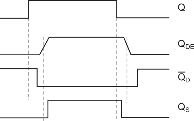
| Figure 2. | The external control-logic signal, Q, splits into two quasicomplementary signals to ensure the internal break-before-make operation of the sample-and-hold amplifier. |
|
The B3 voltage follower serves as a delay line, which, in conjunction with one AND gate and one NOR gate, generates two semicomplementary logic-control signals (Figure 2). Both of these signals, QS and QD/ are thus kept at an inactive low level for a sufficiently long time, before moving to an active high level, providing a break-before-make operation. The input voltage gets tracked at the C1 capacitor with QD/ high, and the last value of this voltage, at the high-to-low transition of QD/ is a sample. The sample, at the instant of the low-to-high transition of QS, appears with a negative sign at capacitor C2 and subsequently at the output.