At least two classic ways exist to address applications requiring sampling of a sum of analog voltages. The most common way is to cascade a classic analog adder and a sample-and-hold amplifier. A classic analog adder is an op amp plus at least three precision resistors. The values of these resistors should be as low as possible so as not to deteriorate the bandwidth of the adder. On the other hand, such low-value resistors dissipate power. Further, the configuration of an adder-sample-and-hold amplifier suffers also from another drawback, which manifests itself when the two input voltages are close in magnitude but of opposite polarity. In this case, even if the magnitude of the input voltages is high, the resulting sum is low or no voltage if the magnitudes of input voltages are equal. Sampling a low voltage usually involves a high relative error of the output voltage because each amplifier has some dynamic errors, such as residual parasitic transfer of charge into the storing capacitor.
Another possibility is to use one amplifier per channel and add their outputs in a classic analog adder. Although this configuration avoids the problem with the high relative error of output voltage when input voltages are similar in magnitude and opposite in polarity, precision resistors in the adder still dissipate power.
 |
|
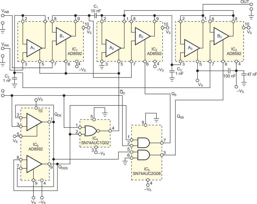
| Figure 1. | The basis of the operation of this circuit is the simultaneous tracking of the VINA and VINB input voltages on the C2 and C1 capacitors, stacking these capacitors within the sample interval, and storing the value of stack’s voltage on the C3 capacitor. |
You can avoid these problems by using the circuit configuration in Figure 1, which uses no external resistors. In the steady state, the internal-tracking interval, the QD internal-logic signal is at an active-high level, enabling the A1, B1, and A2 followers. Thus, the ground-referenced capacitor, C2, charges to the VINA voltage. The lower node of capacitor C1 at Pin 2 of IC2 gets temporarily grounded through the output of the A2 follower while it charges to the VINB voltage at its upper node at Pin 9 of IC1. VINA and VINB are the input voltages at the A and B inputs, respectively.
 |
|
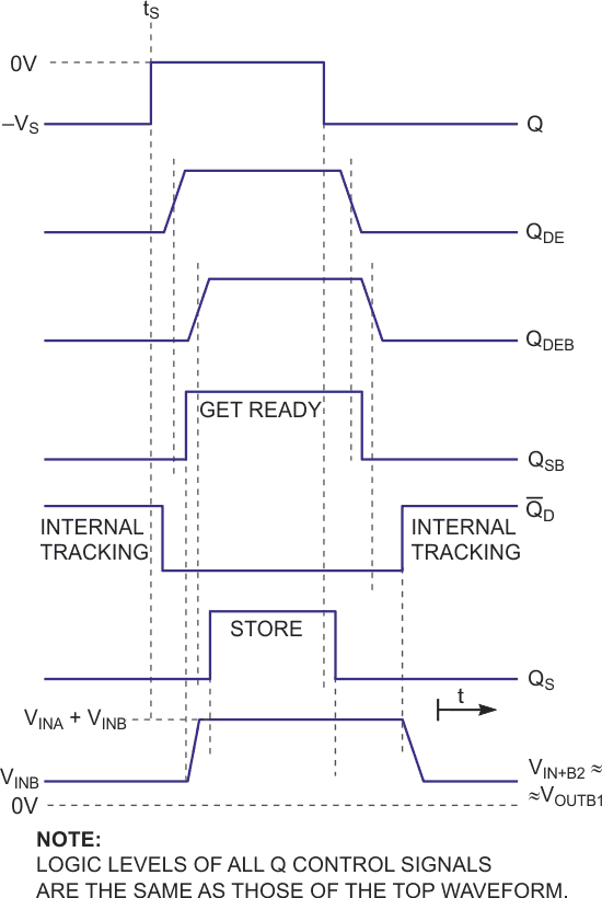
| Figure 2. | The bottom waveform shows that, at the upper node of the C1 capacitor, the VINB voltage appears within the tracking interval, and it rises to the value of the sum of both input voltages within the get-ready interval. |
After a settling period, when all internal logic-control signals are low and all controlled followers are disabled, the QSB control-logic signal goes high. The potential at the lower node of C1 goes from 0 V to VC2(tS) = VINA(tS) because of the enabled B3 follower. VC2(tS) is the value of voltage stored on the C2 capacitor before the transition of the Q signal to an inactive-low level. The potential at the upper node of C1 consequently rises to the value of
VC2(tS) + VC1(tS) = VINA(tS) + VINB(tS),
as the bottom waveform in Figure 2 shows. This trace is the only analog waveform in this figure. The active-low-to-high transition of the sampling-command logic signal, QS, gets slightly delayed with respect to that of the QSB logic signal, suppressing glitches in the output voltage. When QS is high, the sampled voltage of VINA(tS) + VINB(tS), which is present at Pin 7 of IC2, passes through the enabled B2 follower to the C3 capacitor and gets stored there until the next sampling command. The A3 follower serves as an impedance converter. Dual op amp IC6 serves as a tapped delay line, which, in conjunction with one single-NOR gate and one dual-AND gate, derives properly timed internal logic-control signals from the single external logic-control signal, Q.