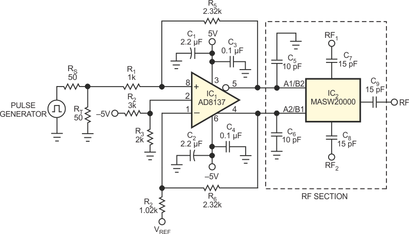
Designed as a high-speed driver for 12-bit ADCs, the AD8137 controls SPDT GaAs (gallium-arsenide) FET-MMIC (microwave-monolithic-IC) and PIN-diode RF switches and thus provides a low-cost and versatile alternative to conventional switch drivers. This circuit achieves typical switching speeds of approximately 7 to 11 nsec, including the propagation delays of the driver and RF load.
 |
||
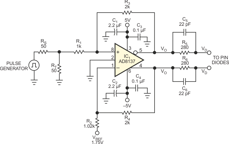
| Figure 1. | ADC driver IC1 converts TTL levels to differential-control signals for GaAs RF switch IC2. | |
The GaAsFET-driver circuit (Figure 1) converts a single-ended, 0 to 3.5 V TTL signal into a complementary, 0 to –4 V differential-output signal. The divider formed by the 50 Ω source impedance, RS, and the input termination, RT, imposes a 50% signal reduction. To compensate, the circuit amplifies its input by approximately 2.3 times to yield the proper output amplitude of 4 V p-p. The circuit also shifts the output level by –2 V to provide the proper GaAsFET bias. Equation 1 determines the output voltage:
 |
(1) |
For a symmetrical output swing, gain-setting resistors R1 and R4 must present the same Thevenin-equivalent resistance. In Figure 1, R4 increases by 20 Ω over R1. This increase compensates for the fact that source resistor RS and termination resistor RT combine in parallel to introduce additional resistance of 25 Ω. Setting R4 to 1.02 kΩ (the closest standard value to 1.025 kΩ) ensures that the circuit will provide approximately equal gains at the differential outputs.
 |
||
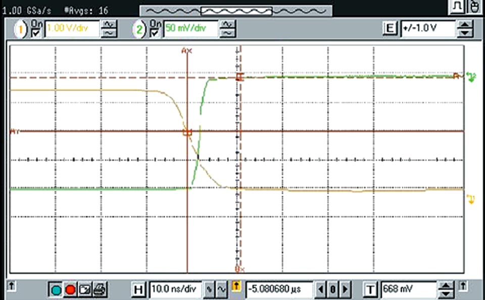
| Figure 2. | Vertical cursors denote GaAs switch turn-on time of approximately 5 nsec. | |
The AD8137's VOCM input (Pin 2) offers a convenient method of shifting the outputs' dc common-mode level. In Figure 1, R2 and R3 form a voltage divider, which sets the dc output level to –2 V. Connecting the AD8137's inverting input to a reference voltage of 1.75 V establishes the midpoint of the input signal and allows for proper switching of the AD8137's input stage.
 |
||
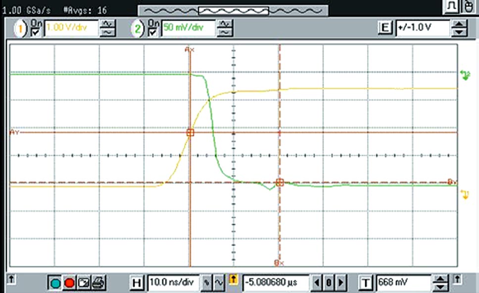
| Figure 3. | Turn-off time is approximately 11 nsec. | |
Figure 2 shows the GaAs FET driver's turn-on switching speed of approximately 5 nsec for isolation to insertion loss – that is, 50% of the TTL input to 90% detected RF. Figure 3 shows turn-off switching speed of approximately 11 nsec for insertion loss to isolation – that is, 50% of the TTL input to 10% detected RF.
 |
||
| Figure 4. | A few modifications convert the circuit in Figure 1 into a PIN-diode switch driver. | |
As Figure 4 shows, with only minor modifications, the GaAs switch-driver circuit can drive PIN-diode loads that require both positive and negative bias currents. IC1's VOCM input connects to ground to provide symmetrical outputs of ±3.5 V about ground and sinks and sources 10 mA of bias current. Altering feedback resistors R3 and R4 to 2 kW provides an output swing of ±3.5 V. Resistors R5 and R6 set the steady-state PIN-diode current, ISS, as Equation 2 shows:
 |
(2) |
Capacitors C5 and C6 set the spiking current IS, which removes stored charge in the PIN diodes. You can optimize a given diode switch's response time by using the AD8137's output slew rate for dV/dt and Equation 3,
 |
(3) |
to calculate spiking current.