Darwin Tolentino and Sandro Herrera, Analog Devices
Analog Dialogue
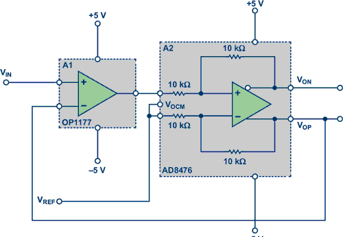
Differential signaling finds useful application in circuits where a large signal-to-noise ratio, high immunity to noise, and lower second harmonic distortion are desired, such as in driving high performance ADCs and high fidelity audio signal conditioning. A related previous article in Analog Dialogue, "Versatile, Low Power, Precision Single-Ended-to-Differential Converter,"1 offers a greatly improved single-ended-to-differential circuit that has very high input impedance, 2 nA maximum input bias current, 60 µV maximum offset (RTI), and 0.7 µV/°C maximum offset drift (Figure 1). The improved performance is achieved by cascading an OP1177 in the feedback loop with the AD8476 that has a differential gain of 1.
 |
||
| Figure 1. | Improved single-ended-to-differential converter. | |
It is desirable, however, in many applications to have a greater output dynamic range, such as in signal conditioning of sensor outputs – for example, temperature and pressure. Being able to also adjust the common mode makes the circuit very convenient in interfacing to many ADCs where the reference determines full-scale range.
 |
||
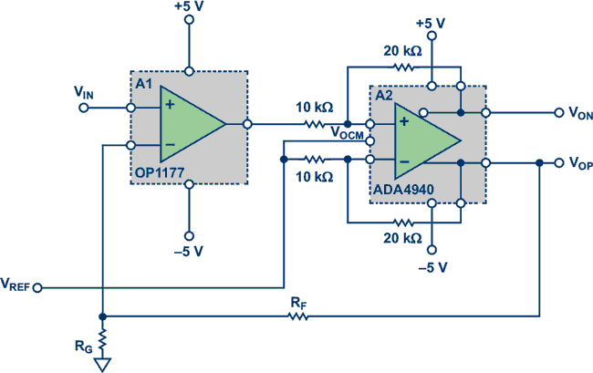
| Figure 2. | Single-ended-to-differential converter with improved dynamic range. | |
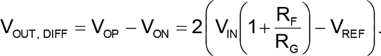
Configuring the differential amplifier inside the loop to a gain greater than 1 increases the output dynamic range of the circuit (Figure 2). The output is given by the following equation:
When RG is left open the circuit has an overall gain of 2. The output of A1, OP1177, is given by the following:
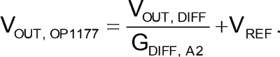
Notice that the VREF is always added to the output of the OP1177 limiting its output headroom. In most applications the VREF (the output common mode) is set at the center of the supplies for maximum output dynamic range. A differential amplifier inside the loop configured at a gain greater than 1, such as the ADA4940 in Figure 2 (gain of 2), reduces the output voltage of A1 by a factor of A2's differential gain and helps avoid saturating the output of A1. Because the OP1177 has a typical output swing of 4.1 V at ±5 V supplies, the differential output voltage swing of the circuit in Figure 2 is about ±8 V at VREF set at 0. Configuring A2 to a gain of 3 further improves the output dynamic range and achieves the maximum output swing of the circuit. Another amplifier, the ADA4950 with available gains of 1, 2, and 3, may also be suitable for A2.
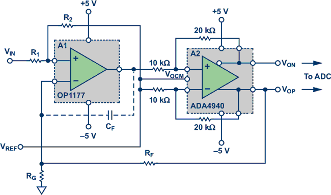
Adjustable Output Common Mode
The circuit can be modified to make the output common mode adjustable and independent of the common mode of the input signal. This adds great flexibility and convenience for single- supply applications where the input is referred to ground and is needed to be converted to a differential signal with an elevated common mode for ADC interfacing.
This can be accomplished by adding two resistors at the input R1 and R2, where R2 is tied to VOCM. If desired, using a dual version of the input amplifier A1, the OP2177, allows for the second amplifier to be used as a buffer to the input for very low input bias current.
 |
||
| Figure 3a. | Improved single-ended-to-differential converter with adjustable common mode. | |
In the circuit in Figure 1, the input is referred to VREF. Referring to the circuit in Figure 3a, the input is referred to ground taken directly and converted to differential output. The VOCM can now be adjusted to shift the common-mode output while the input remains referenced to ground. The VOCM can be tied to half of the reference or the midscale of the converter. The VOCM basically acts as another input along with VIN. The values of the resistors should be chosen such that
By superposition, when VIN is 0, the output is forced at the same value as VOCM. And since VOCM is the value that sets the output common mode, the differential output is zero. If R1 = RG and R2 = RF, the output voltages are given by:
Bandwidth and Stability
 |
||
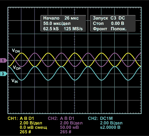
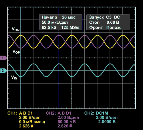
| Figure 3b. | Input and output plots, VOP in red, VON in yellow, and input in blue. Common mode is at 0 V. |
|
 |
||
| Figure 3c. | Input and output plots, VOP in red, VON in yellow, and input in blue. Common mode is at 2.5 V. |
|
The two amplifiers form a composite differential output op amp in a servo-loop configuration. The OP1177/OP2177's open-loop gain and the differential gain of the ADA4940 combine for the total open-loop gain of the circuit that defines the overall bandwidth of the circuit. Their poles combine for additional phase shift in the loop. A higher gain for A2 reduces its bandwidth and may affect the stability of the overall circuit. The circuit designer must check the overall circuit frequency response and assess the need for compensation. A rule of thumb is that the combined open-loop gain over frequency must cross the unity gain at –20 dB/decade roll-off in order to ensure the stability of the feedback system. This is particularly more important in applications with the minimum gain (gain of 2) where the loop gain is at maximum and has the worst phase margin. A higher overall gain also improves stability by decreasing the bandwidth and increasing the phase margin of the feedback loop. Because the loop gain is decreased, it crosses the unity gain at a lower frequency. The loop gain is given by:
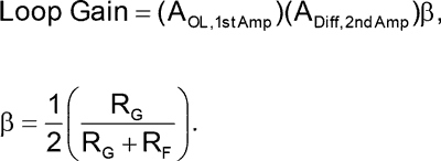
The feedback factor β has ½ in the term because the output is differential and the feedback is taken only from one of the differential outputs. The ADA4940 has a bandwidth of 50 MHz at a gain of 2, while the OP1177 has a unity-gain bandwidth of about 4 MHz. The circuit in Figure 3 is stable with a bandwidth of about 1 MHz, limited by the OP1177 and the closed-loop gain. As pointed out in the previous article, when the stability condition cannot be met using different amplifiers, a bandwidth limiting capacitor can be used as shown in Figure 3a. The capacitor forms an integrator with RF inside the feedback loop and limits the bandwidth of the overall circuit to
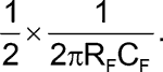
The capacitor and feedback resistor can be chosen such that the overall bandwidth is limited by the equation above.
Reference:
- Herrera, Sandro and Moshe Gerstenhaber. "Versatile, Low Power, Precision Single-Ended-to-Differential Converter." Analog Dialogue, Volume 46, Number 4.