The function generator is a generic measurement equipment to generate test signals. Most function generators can generate a sine, square and/or triangle wave and high end equipments support arbitrary waveforms and have multiple channels. The simple function function generator can be built easy, so that there are many home-build projects from old days. The method of waveform synthesis can be divided in two categories, one is analog synthesizing method and the other is digital synthesizing method.
As for analog synthesizing, wien bridge oscillator or traditional function generator IC ICL8038 are often used for home-build equipments. These analog method can be realized in very simple circuit, however, there are problems on stability, accuracy and reproducibility.
The digital synthesizing method have grown recent days. It synthesizes the waveform data in digital processing and the data is converted to analog signal with a DAC. This is the method called DDS. Because it generates the waveform with a digital circuit, it has very good stability, accuracy and reproducibility compared to the analog method, and can be fully controlled by a software. This is a project that to build the DDS function generator.
The Principle of DDS
Continuous signal and Discrete signal
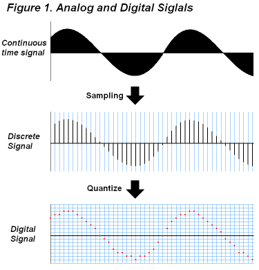
When process a time-continuous signal with a digital circuit, it is sampled at regular intervals and then quantized to convert a digital data like shown in figure 1. The values of the sampled signal is exist at only sampling points and there is no valid data between them. This form of signal is called discrete signal and thus digital signal process handles signals in form of discrete signal.
The discrete signals can be handled as equivalent to time-continuous signals, however, there are some consideration to be given to its characteristics. For example, there is no waveform data between the sampling points, variation of waveform faster than sampling rate cannot be expressed correctly in the discrete signal. The frequency components that can be expressed correctly become eaual or less than fs / 2 [Hz] at the sampling freqency of fs [Hz]. This limit is called nyquist frequency. Threrfore, higher sampling rate increases the processing freqency bandwidth. However, the system resource, shch as processing speed and data storage area, is limited, so that a minimal sampling rate for each application is chose in trade-off between the cost and the performance.
When think about the discrete signal as "impulse signal in freqency of fs that modurated by input signal", its characteristics, such as frequency spectrum repeated infinitely, will able to be recognized easy.
Digital synthesizing of a waveform
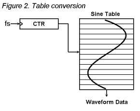
When synthesize a waveform in digital signal processing, it follows the process described above in reverse order, synthesize a digital signal (waveform data) for each sampling point and convet it to analog signal with a DAC. For example of synthesizing a sine wave, the instantaneous value e of the sine wave is as follows:
e = Ep * sin(θ) = Ep * sin(ωt) = Ep * sin(2πft) ---(1)
where Ep is the peak value, ω is the angular speed [rad/sec], f is the freqency [Hz] and t is the past time [sec]. The sine wave data can be synthesized when calcurate the values for each sampling point with the time t. Ofcourse what waveform f(t) other than the sine wave that is function of t is in the same way.
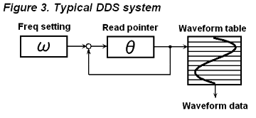
Practical DDS system
|
|
Considering the specification
I determined the specifics of the function generator as follos:
- Generate waveforms in DDS method.
- Used for measurement of audio system
- Fully controlled with a μC and eliminate analog volumes.
- Can generate arbitrary waveforms other than sine wave.
The reason why I chose these aims is that, 1 is the aim of this project, 2 is that the planning use, 3 is that analog volume is not accurate.
How to realize the DDS
There are two methods to compose the DDS system, the one is to build with only hardware logics, the other is software processing with DSP or MCU. The hardware method uses a DDS-IC or a PLD. The DDS IC is designed for digital communication, it cannot generate arbitrary waveform, has not a digital attenuator and the vertical resolution is not sufficient for audio applications; therefor the DDS-IC cannot be used for this project. The PLD-DDS will able to solve these ploblem. However a MCU is used at least for system control, so that I considered that if a generic MCU can realize a DDS or not.
For audio measurements, 16 bit vertical resolution and samplig rate of 100 ksps will be required at least. As the result, I estimated that the DDS can be processed with an AVR with load ratio of about 80 percent. This is the field of DSPs or 32-bit MCUs but it can also be done with an AVR, such the expensive processors are not needed for this project.
Output
I used a stereo DAC that digged out at junk box. This gives two individual waveform outputs. It will enable the experiments on phase, complex signal, and IMD test.
User Interface
A 20 column by 4 row LCD module is used for display. Because the function generator has two output channels, there are many parameter to be displayed, so that it requires four rows at least. For user input, four arrow buttons and a rotary encoder are used. The waveform is loaded from a memory card.
Hardware
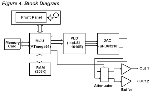
Figure 4 shows the functional block diagram of the function generator. Follows are descriptions for each block.
Circuit diagram (controller) | Circuit diagram (analog part)
Microcontroller
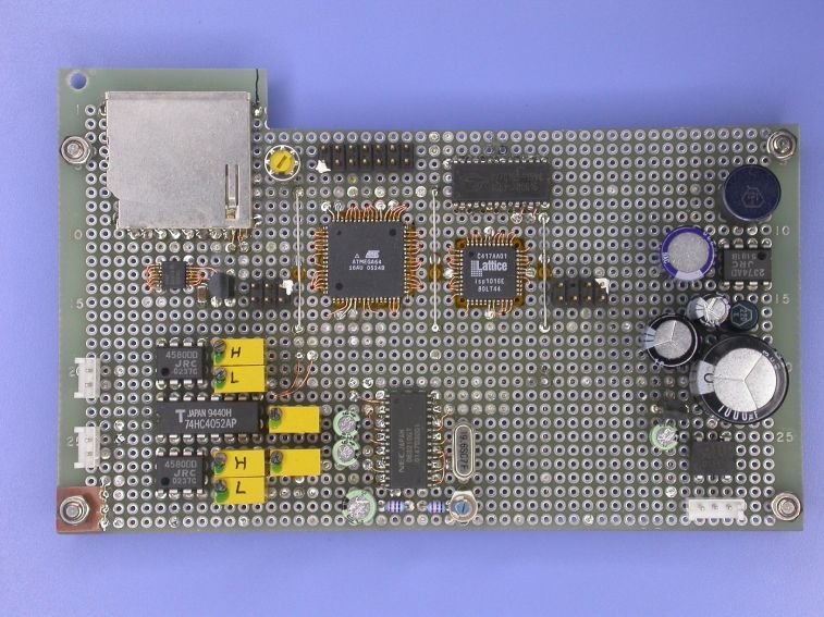
An ATmega64 is used for the controller. The MCU has an external memory interface, it benefits the applications that require a certain memory. The waveform data is loaded from a memory card and stored it to the wavetable located in the 256 Kbit external memory. The wavetable, 16 bit word, 8192 samples and two channels, fits to the entire memory. The system clock is supplied from DAC. The frequency exceeds maximun allowable working frequency of the MCU, however it works with no problem.
PLD
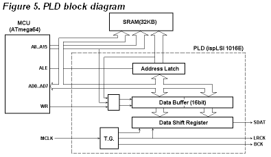
Figure 5 shows the functional block diagram of the PLD. A Lattice ispLSI1016E that I had in my parts box is used. It will able to be replaced by any CPLDs that have 64 macrocells. It is used mainly as a serializer to send the waveform data to the DAC. The glue logic, required to attach an external memory to the AVR, is also incorporated into the PLD. The LRCK to the DAC is used to a sampling interrupt to synchronize DDS process and DAC.
DAC
An NEC μPD63210 is used. This is a resistor string 16-bit stereo audio DAC with built-in oversampling digital filter. The digital filter reduces aliasing noise near input signal band, so that post filter can be simplified and the waveform can be represented without any distortion upto near nyquist frequency. The μPD63210 can work at 96 kHz input sampling rate, so that audio bandwidth of 40 kHz that two times higher than generic audio frequency can be represented. Ofcourse any other audio DAC that supports 96 kHz samplig rate will able to be used. In this project, the master clock to the DAC is changed to adjust the fundamental frequency to 12.5 Hz (@8192pts), and running the DAC at 102.4 ksps. The power line to the DAC must be kept clean, or it causes a spurious on the output signal, so that power supply is created with a series regurator and supplied to AVDD and DVDD via LC filter individualy.
Analog Part
The offset voltage on the analog output is canceled, selected two atteuation ratios (1/1 and 1/16) and buffered it to drive a load. The reason, output level is controlled at digital part but using an analog atteuator, is from very wide output voltage range and to prevent insufficient vertical resolution at low voltage range.
Software
DDS process
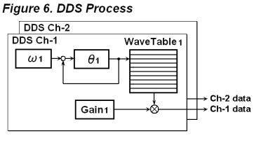
Figure 6 shows the data flow diagram for DDS process. This process is driven in sampling interrupt by LRCK as follows:
V1 = WaveTable1 [(θ1 += ω1) % 8192] * Gain1;
V2 = WaveTable2 [(θ2 += ω2) % 8192] * Gain2;
The results V1 and V2 are sent to the DAC via a serializer. The DDS registers ω and θ are 13.7 fixed point registers. This process must be processed in sampling rate of 102.4kHz, and the given CPU clocks between each sample becomes only 192 clocks. The DDS routine with asm code might or might not able to execute within this time.
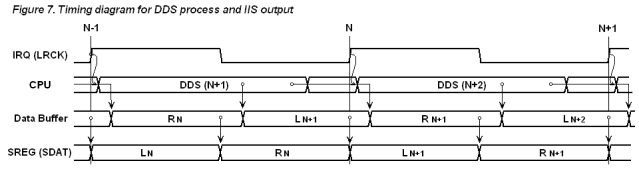
As the result of some trials, it achieved 157 CPU clocks for a sample process. The load ratio becomes 82 percent and the CPU power of about 3 MHz remains for foreground process under running the DDS. Figure 7 shows the timing diagram of the DDS process and output data. In the program code, static register variables are defined to eliminate time loss due to save/restore data at entry and return of ISR. The interrput response time of the DDS process must be minimized to keep the continueity of the waveforms, so that another ISRs allow nested interrupt to give the highest priority to the DDS process. However these considerations are not applied in file access module because DDS is always stopped during file access (loading waveform).
Managing Waveforms
The waveform data is stored to a memory card as generic csv file. The data format is: two columns (ch1, ch2) for each line, 8192 lines, the range of the sample value is -32767 to 32767 integer and the value is normalized in justifying peak level to 32767 or -32767. These files are managed with an index file for displaying waveform name and listing order in the selection menu.
The waveform files are supplied in csv format, however the waveform change takes about 2 seconds due to an overhead on text processing. To solve this problem, the loaded waveform and its characteristics (crest factor, and peak to peak level) are cached into a binary file (.bin) and the chache file is loaded next time.
User Interface
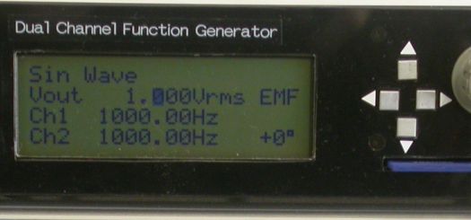
The photo placed in top to this page is the front panel. The parameters on the synthesizing waveform, waveform name, output voltage, ch-1 frequency, ch-2 frequency and ch2 phase, are displyed in the LCD. These parametres can be changed with arrow buttons and a dial. When change the waveform, select with the dial and change with left arrow button.
That photo shows the phase control mode. In this mode, ch-2 frequency tracks ch-1 frequency change and the phase delay can be changed in resolution of 1 degree. When ch-2 frequency is changed, it goes to dual-tone mode. In this mode, phase display becomes "***" and the frequency can be set each channel individualy. When phase delay is changed, it returns to the phase control mode and ch-2 frequency is fixed to ch-1.
The output voltage is displayed in EMF voltage because most audio systems accept the input siglans in high input impedance. To change the unit of output voltage, move cursor on the voltage unit and select with a dial. The dBm form is based on load impedance of 600Ω, so that 0 dBm becomes 775 mVRMS. When attach a 600Ω load, the output voltage lowers 0.7 dB due to Zo (50Ω) and the load resistance. The maximum output voltage is approx. 5 VRMS, however allowable voltage is limited by the crest factor of the selected waveform.
Building the circuit board
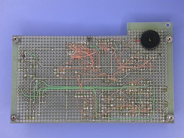
This is a mixed signal system, the digital part and the analog part are exist on the same circuit board. The considerations of the mixed signal circuit are required to the parts layout and grounding. But it is not that difficult when it is done under generic considerations.
Adjustment
After the MCU and PLD are programmed, confirm each function that it is works fine and the waveform is appeared or not. And then provide an AC volt meter to be referenced.
First, stop waveform output and adjust VR1 and VR2 as offset voltage at attenuator switch becomes zero volt. Next, output a 5 VRMS sinewave and adjust VR3 and VR5 as the output voltage at output terminal becomes 5 volts, and then adjust VR4 and VR6 as output voltage changes continueously when attenuation ratio is changed (U5-10 changes L to H) around 0.34 volts. Final, ajust VC1 as master clock frequency becomes 19,660,800 Hz. However the VC1 can be ommited because the accuracy is sufficient for audio measurement even if it is not adjusted.
Results and Cosiderations
Waveforms
These are the waveforms in phase controlled mode and dual-tone mode. Also a complex signal can be generated because there are two waveform tables for each channel individualy. The frequency can be changed instantly with continuous phase. The waveform can be changed in 50 milliseconds by effect of the binary cash. When output a squarewave, ringings that specific to digital filter appear on the edges. When frequency is set to 40 kHz sinewave that near the nyquist freqency, the sampling points that rising edge of LRCK becomes very coarse. But the waveform still represented as a smooth sinewave by 8th order oversampling digital filter.
Audio Performance
I measured the audio characteristics. The THD+N varies cyclically between 0.01% and 0.03% due to rounding error of digital attenuation. The SNR was 85 dB at 1 kHz, 1 VRMS. Note that these values are the results under applying JIS-A filter. It seems a decent performance when took the raw performance of the DAC into consideration.
The user interface is the most impotant device that affects the usability. In this project, an LCD display, four arrow buttons and a jog dial are used and it acheved very good usability.
Notes
|
Specification of the DDS function generator |
|
|
Main ICs |
MCU: ATmega64 (ATMEL) |
|
DDS function |
Number of channels: 2 |
|
Analog output |
Zo=50Ω, 2ch |
|
Frequency range |
0.01Hz - 45,000.00Hz (0.01Hz step) |
|
Voltage range |
0.001 - 20.000VRMS (0.001VRMS step) |
|
Ch2 phase |
-180° - +179° |
|
User interface |
Character type LCD module (20C,4R), |
|
Waveform recording media |
MMC or SDC |
|
Power supply |
AC line |
Diagrams and Photos
 |
 |
|
| Circuit board (top) | Circuit board (bottom) | Inside the case |
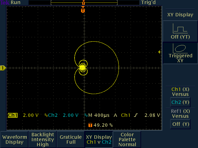 |
| X-Y display of a complex signal |
References
- Motokazu Imamura, Fundamental of video signal and its operation,CQ publishing, ISBN4-7898-3624-X