Horst Koelzow
EDN
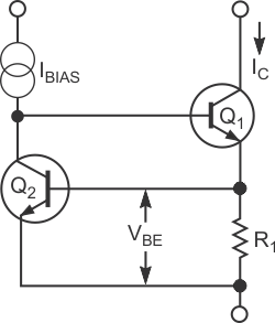
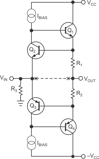
The basis for this Design Idea is a classic two-transistor current source (Figure 1). Current through R1 depends only on the VBE (base-emitter voltage) of Q2 and on the value of R1 itself. The VBE of Q1 has no impact on the output current. Typically, this circuit finds use as a steady current source or as a limiter. The circuit forms the amplifier for the upper, positive half of the signal. Adding a complementary stage for the lower, negative half of the signal completes the buffer (Figure 2). The emitters of Q2 and Q3 become the input for the circuit, and the junction of sensing resistors R1 and R2 is the output. R3 is an input-termination resistor that sets the output quiescent voltage. You can replace the bias sources (current sources in the figures) with resistors.
 |
||
| Figure 1. | This classic two-transistor current source commonly finds use as a steady source of current or as a limiter. |
|
At the quiescent, 0V-input-voltage operating point, both halves of the circuit run at maximum current, and both the input and the output are at the same potential. When you impress a voltage on the input, you inject current into the Q2–Q3 emitter node. From there, current can go up into base of Q1 or down into base of Q4. The output voltage relative to the input voltage determines the direction of the injected current. If the input voltage is positive, it has no effect on the upper half because it is already limiting. It can, however, reduce drive current in the lower half, resulting in a reduction of lower output-drive current. Reduction of lower side output current results in a rise in output voltage. In short, an injected signal current "unlimits" the stage of opposite polarity.
 |
||
| Figure 1. | Adding another stage to the current source allows the circuit to function as a buffer. |
|
At first glance, the circuit appears to have unity gain. But, because Q2 and Q3 sense the tops of R2 and R3 and not circuit output, R1 and R2 are effectively in series with the output load. If the load's impedance, RLOAD, is small, the circuit gets significantly loaded down. However, as long as the input stage does not clip, the circuit does not become distorted. The source driving the buffer stage sees
hFE(Q1) × (R1 + RLOAD) Ω,
where hFE is forward-current gain.
Q2 and Q3 are common-base stages. Their purpose is to translate input voltage to the bias voltage that Q1 and Q4 require. This voltage-translation action allows direct substitution of other devices, such as MOSFETs or Darlington transistors.