Michael Gurovich, USA
In today’s age, measuring devices with digital indication of measurement results, such as Digital Calipers, Micrometers, Dial Indicators (DI), are becoming widely popular. Most of these devices also have a port for outputting data to an external device for storage or analysis. Usually it is a serial data output interface, using the DT data line and the CLK strobingclocking signal line. When trying to read such a signal in the usual way, an incompatibility problem arises, since the output data has non-standard voltage levels and a different logical format.
This article describes one of the ways to read and transfer information from the DI to a PC.
In this project, the task is to automate the process of measuring the amplitude of vibrations of the working end of the sonotrode in an ultrasonic metal welding system. During ultrasonic welding, the sonotrode oscillates at a frequency of about 20 kHz and with amplitude of 20 to 40 microns. This amplitude measurement automating during welding was this project’s goal.
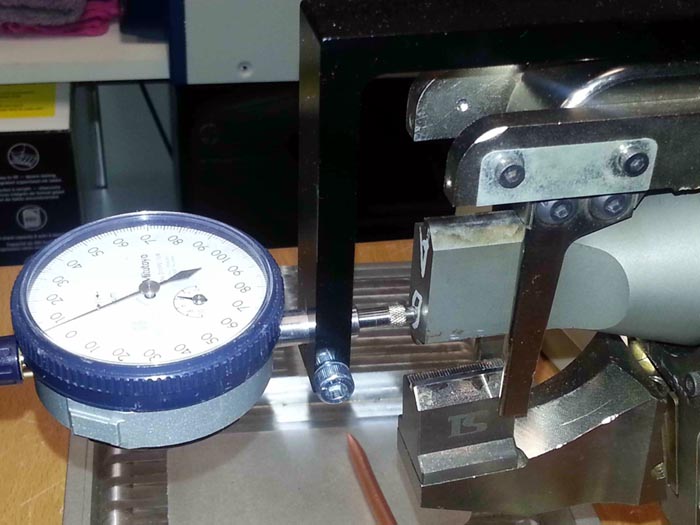
Initially, to measure the vibration amplitude of the sonotrode, a mechanical DI was used. During welding, the maximum needle deflection was noted and then the instrument reading at rest was subtracted from this value. The difference of these two values is equal to the amplitude of oscillation of the sonotrode.
 |
||
| Figure 1. | Mechanical DI when measuring the amplitude of oscillations of a sonotrode. |
|
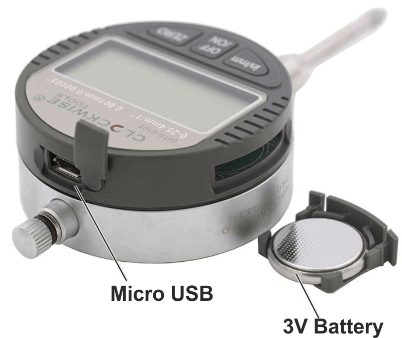
In this project, a digital DI oftypeClockwiseTools DITR0105 was used.
 |
||
| Figure 2. | Electronic DI ClockwiseTools DITR-0105 | |
This device has an LCD for result-indication and a port for outputting measurement data in the form of a serial interface.
In the process of working with that DI , it turned out that the output port has three lines - the Ground( GRND), the Data (DT) and the Clock line (CLK).
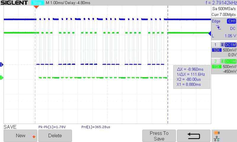
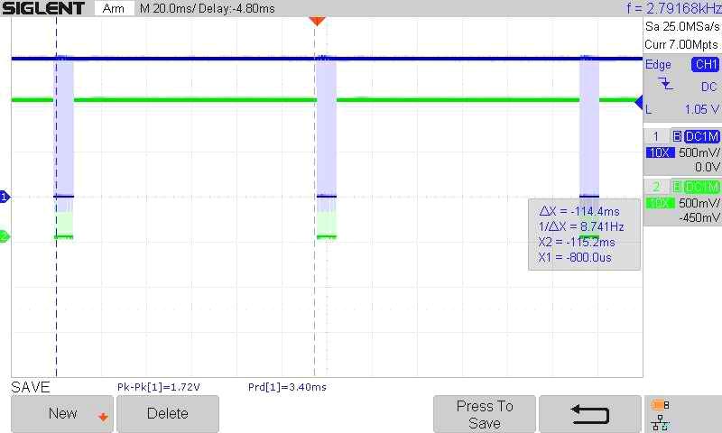
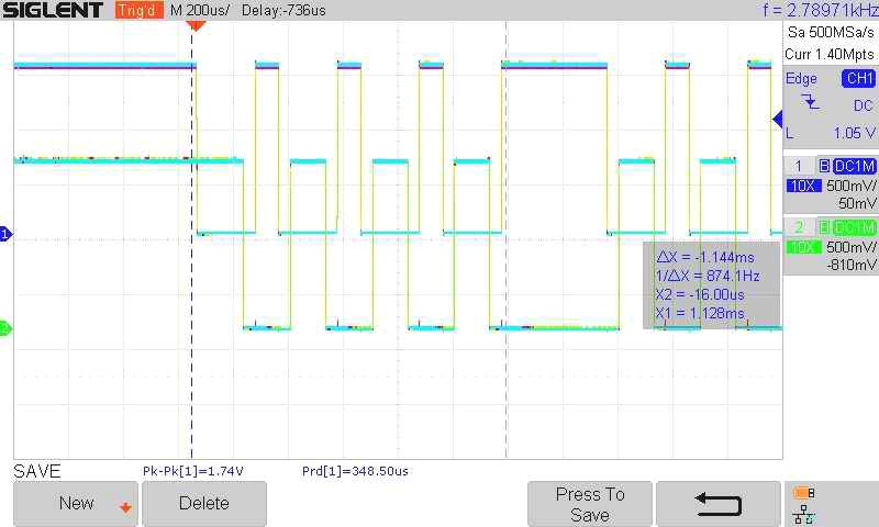
Signals shapes of these lines are shown in Figures 3, 4, and 5.
 |
||
| Figure 3. | One complete DI data packet. | |
 |
||
| Figure 4. | Several packets of data at the output of the DI. | |
 |
||
| Figure 5. | A few bits of data at the output of the DI. | |
When analyzing the situation, it became clear that to transfer this information to a PC, two problems had to be solved:
- The conversion / change of DI signal levels from non-standard levels (Low = 0 V, and High= 1.5 V) into TTL levels.
- TheDI data comesout in an unknown/nonstandard format and must be decoded / convertedinto a format compatible with a PC, for example RS232.
The first problem was solved by using a level shifter, which generates TTL level signals in order toapply them to digital uPinputs.
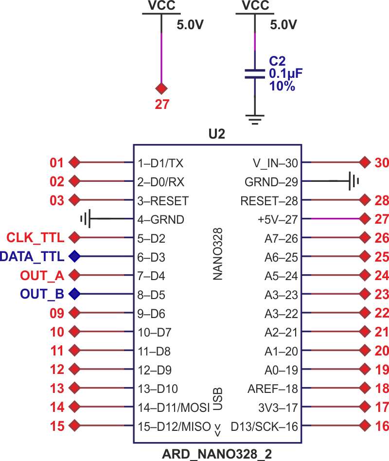
The second problem was solved using the uP(ArduinoNano), which receives TTL signals to its inputs, processes them, and generates output data in the RS232 format (more precisely, the logical output format is RS232, but physically the signals come to the PC input over a standard USB port).
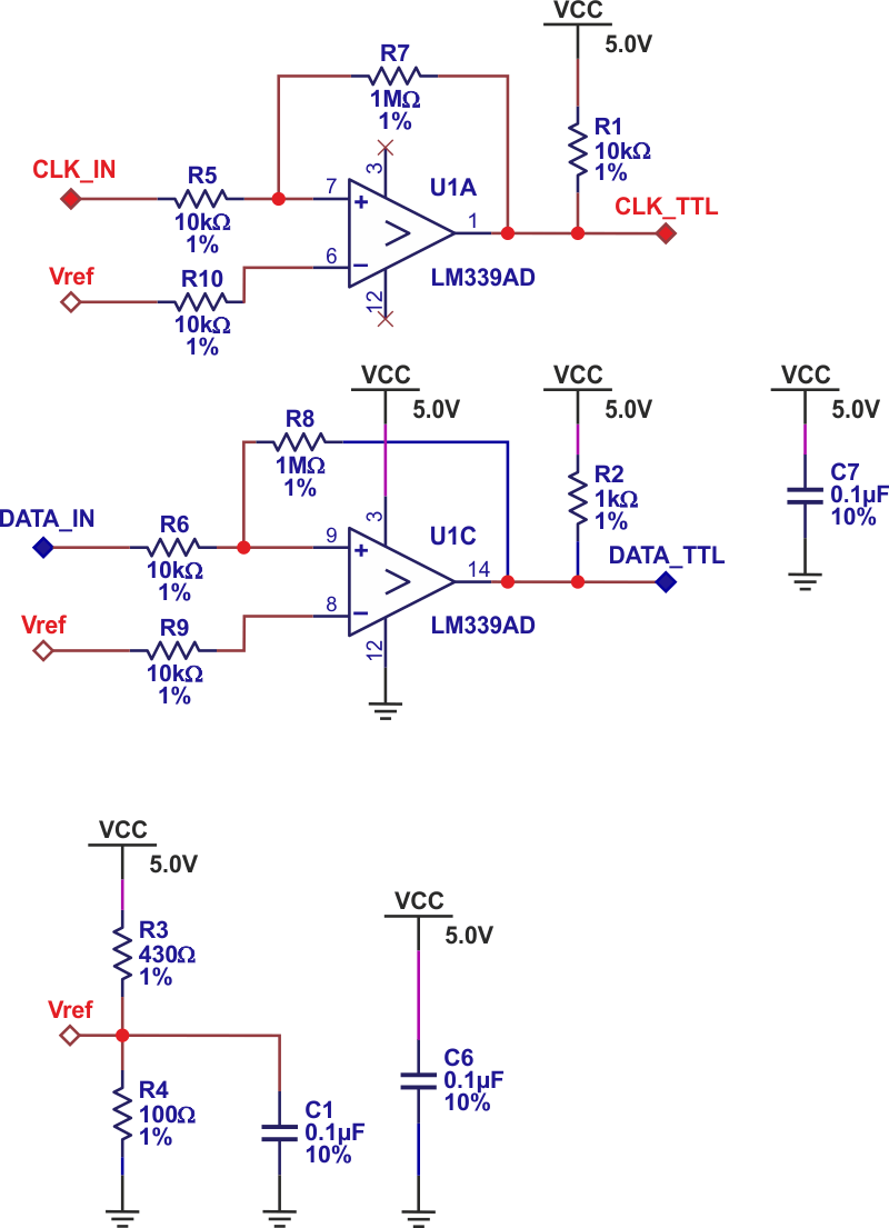
First, let’s discuss the solution to thefirst problem. As noted above, DIsignals have levels of 0 and 1.5 volts. A circuit based on the LM339AD comparator was used to generate TTL level signals (two channels out of four were used). One channel processes the DT signal, the second one - CLK. The principle of operation of the circuit is simple - a reference voltage of approximately +1 V is applied to the negative inputs of both comparators. The positive inputs receive signals from the DI. The outputs of the comparator follow the movement of the input signals, but already with TTL levels. These output TTL signals are fed to the digital inputs of the uPfor further processing.
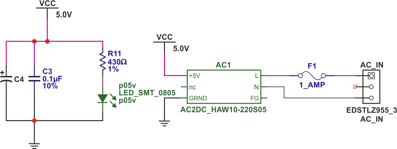
The electronics of the project can be divided into three blocks- Analog Part, uP and Power Supply. Their schematic diagrams are shown in Figures 6,7,8. PCB shown in the Figure 9.
 |
||
| Figure 6. | Analog part of the project. | |
 |
||
| Figure 7. | Microprocessor Arduino Nano. | |
 |
||
| Figure 8. | Project Power Supply. | |
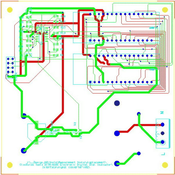 |
||
| Figure 9. | Project PCB (top layer is green, bottom is red). | |
Gerber files are attached to the article.
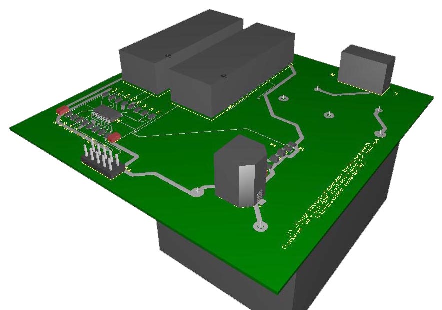 |
||
| Figure 10. | View of the assembled module. | |
Note - there are several components in the project that are not used in this version and are included in the project for future useonly.
These are the third and fourth comparators, resistors R12 - R19.
Additionally, we have added a second uPin the project, in order to have a second footprint on the PCB for debuggingpurposes.
All these additional components are included in PCB and Gerber’sfiles, but are not installed or used in this project.
The solution to the second problem — processing input signals and generating output data in the RS232 format — has been done using the Arduino Nano uP and C++ code.
Description of the algorithm and code.
As noted above, the uPshould perform two tasks -
- decode input pulses
- generate data for transfer to PC.
When analyzing the input pulses, we found the following -
- Data is received in sequential code
- Packets arrive at a frequency of approximately 10 Hz,
- The length of one packet is 9 ms,
- DT line reading occurs on the rise of the CLK signal.
- Bits are packed in groups of 4 and there are 6 such groups in each packet, thus the full data packet contains 24 bits,
- Low bit comes first, high bit comes last.
- The first 16 bits contain the binary code of the measurement result, the last 8 bits contain information about the sign of the result (bit 20) and the measurement unit (bit 23).
Note - in this version of the code, information about the measurement units is ignored, since it is assumed that the DI operates in the metric system.
The uPconstantly checks the state of the CLK input, and as soon as a pulse arrives, the uPreads the state of the DT line and stores the read value in a 24-byte data buffer.
After each read pulse, a wait timer is activated. If after the last received pulse a time longer than the specified time has passed, the last received pulse is considered as the last one in the previous packet and the next received pulse will be considered as the first one in the next packet. This algorithm allows us to determine the beginning and end of data, starting from any time point and loses only the very first packet. All subsequent packets, starting with the second one, are received and decoded without problems.
So, as soon as the uPfound that the last packet pulse has been received and recognized, the following sequence of actions is performed -
- The bits of the buffer are reversed (the order of the bits changes to the standard - the most significant is on the left, the least significant is on the right),
- The low 16 bits are converted from binary to decimal format,
- The sign of the number is decoded (bit 20),
- A number is formed with a sign
- This number is sent to a PC using a USB port and RS232 protocol,
- The buffer is reset to receive the next packet.
C ++ source code is included in SW02a.ZIP file
This is what this project looks like in action:
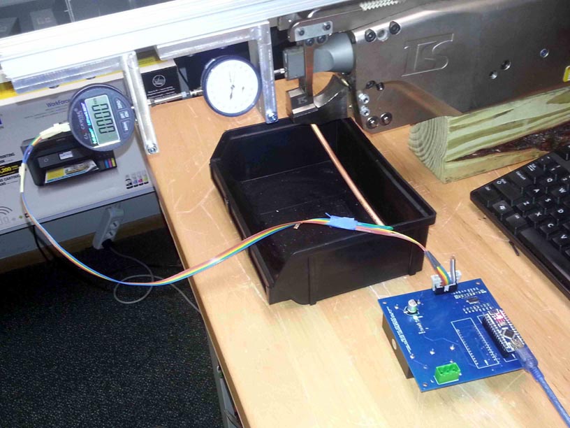 |
||
| Figure 11. | Project in action - general view. | |
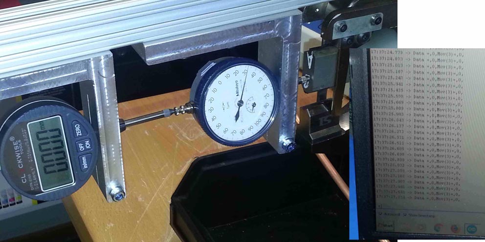 |
||
| Figure 12. | Project in action - measurements of the state of rest and data on the PC screen | |