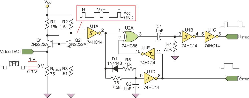
By providing simultaneous output of composite video, this video-sync separator design offers an alternate method for providing horizontal (H) and vertical (V) sync signals that support RGB video output to VGA-interfaced computer monitors.
Often times, there aren’t enough unused GPIO pins on a digital signal processor to provide individual horizontal (H) and vertical (V) sync signals that support RGB video output to a typical VGA-interfaced computer monitor. However, with the simultaneous output of composite video available, this solution achieves the same result, but at far less cost than commercial off-the-shelf ICs (Fig. 1).
 |
||
| Figure 1. | The sync separator consists of a small handful of standard, inexpensive components, with U1D functioning as an integrator while U1B and U1C act as a differentiator, to separate the composite signal's H- and V-sync components by both their amplitude and width. |
|
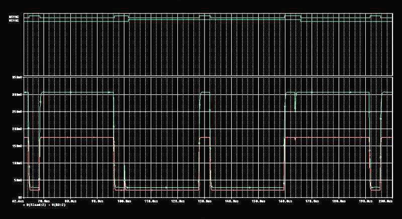
Most video DACs provide a current-output signal, which creates the video voltage across a nominal load resistance (typically 75 Ω, the parallel combination of local and remote 75-Ω terminations) to ground. In this case, the sync-signal tips are at 0 V, the video black (blanking level) is at 0.3 V, and the maximum (white level) of the video signal is at 1 V (left side of the figure). A signal chart shows the composite video sync signal input, the comparator reference level at the emitter of Q2, and the resulting HSYNC and VSYNC TTL-level outputs (Fig. 2).
 |
||
| Figure 2. | The lower green trace is the composite sync input from the video DAC (for clarity, video signals from 0.3 to 1 V are not included). The red trace is the voltage reference level set by the on-current through Q2 into R3; the top two traces show the resulting TTL logic-level H- and V-sync outputs. |
|
Q1 and Q2 implement a temperature-compensated comparator, capable of resolving voltage levels in the millivolt range referenced to ground. R1 provides base bias for Q2 and should be sized so that the current in RLOAD doesn’t excessively offset the black level. The value shown creates only +2 mV offset in RLOAD. Q1’s VBE matches the value of Q2. Thus, if Q1’s emitter goes below Q2’s emitter voltage, Q2’s base current is shunted to RLOAD, turning Q2 off and providing a positive-going signal in response to the negative-going composite sync signals. Signal levels above the comparator trip-point level – 160 mV in this implementation – saturate Q2.
The output at the Q2 collector swings from near-ground to VCC, which is sufficient to drive the inputs of most TTL and CMOS logic families. U1A inverts and buffers the signal for driving the ensuing differentiator and integrator stages. U1D and associated components R5, C2, and D1 form an integrator, whose time constant results in a 64-μs, positive-going, sync-pulse output that meets the VGA specification for VSYNC. The integrator ignores the inverted HSYNC pulse in the middle of the composite video VSYNC pulse. This is visible in an amplified and inverted form at the collector of Q2 in the schematic diagram and the signal chart.
U1B and U1C form a differentiator that also acts a positive edge-triggered pulse generator. The output pulse width is nominally 4 μs to comply with the VGA standard. Without U2A and U1E, the HSYNC pulse at the falling edge of the VSYNC pulse would be missing. Including these two circuit elements restores this HSYNC pulse with minimal timing errors. The HSYNC pulse width at the leading and trailing edges of the VSYNC pulse are approximately 1 μs wider than the other pulses; otherwise, the leading-edge timing is the same as that of the input composite-video signal. The delay from input to output in the HSYNC path is about 124 ns, which is well within the ability of most monitors to compensate and provide properly centered video on the screen.
This design will operate at either 3.3 or 5 V, although R1, R2, and R3 values may need adjustment to provide the proper comparator level when operating at 3.3 V (the values shown are optimized for 5-V operation). Note that 100-Ω damping resistors are commonly placed between the HSYNC and VSYNC outputs and the connections to the VGA connector. Logic types aren’t critical, and substitution of the active components shouldn’t materially affect operation.