Using a bootstrapping scheme with a JFET can enhance a photodiode’s ac response, but adds unwanted dc voltage. Remedy that problem with a matched dual-JFET.
Linear Technology has a good application note [1] about using a discrete JFET to improve the ac response of a large-area photodiode. The circuit uses the JFET as a voltage follower on the cathode side of the photodiode (Fig. 1). This nulls the effect of the diode's internal resistance and capacitance. If there’s no voltage change across the diode, the resistance and capacitance have no effect on the circuit. And the photocurrent generated by the diode is unaffected by the bootstrapping action of the JFET.
 |
||
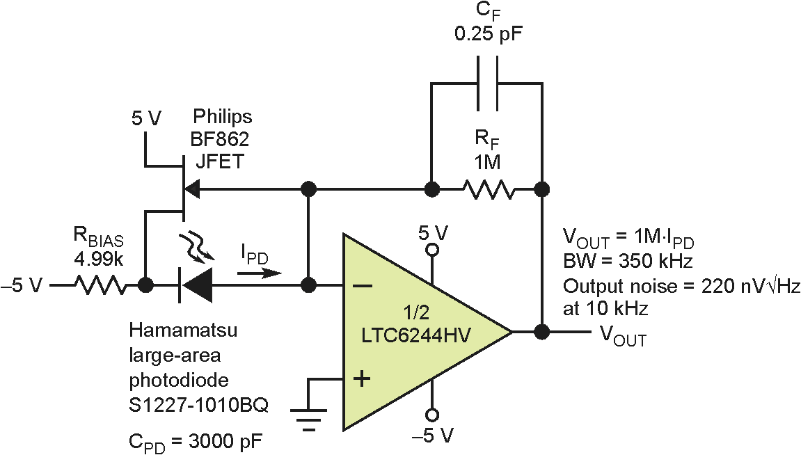
| Figure 1. | This circuit uses a JFET to bootstrap the cathode of the photodiode. It eliminates the effect of diode resistance and capacitance. This improves bandwidth and reduces noise, but puts a dc voltage across the diode. |
|
The bandwidth of the JFET is greater than the amplifier, so the bootstrapping action extends to the unity-gain bandwidth of the amplifier. The bootstrapping makes the photodiode's 3000-pF internal capacitance appear to be zero at the amplifier input. Removing this capacitance will eliminate the input pole, or lag, from the circuit and allow you to use a smaller compensation capacitor. This will extend the frequency response of the circuit (Fig. 2).
 |
||
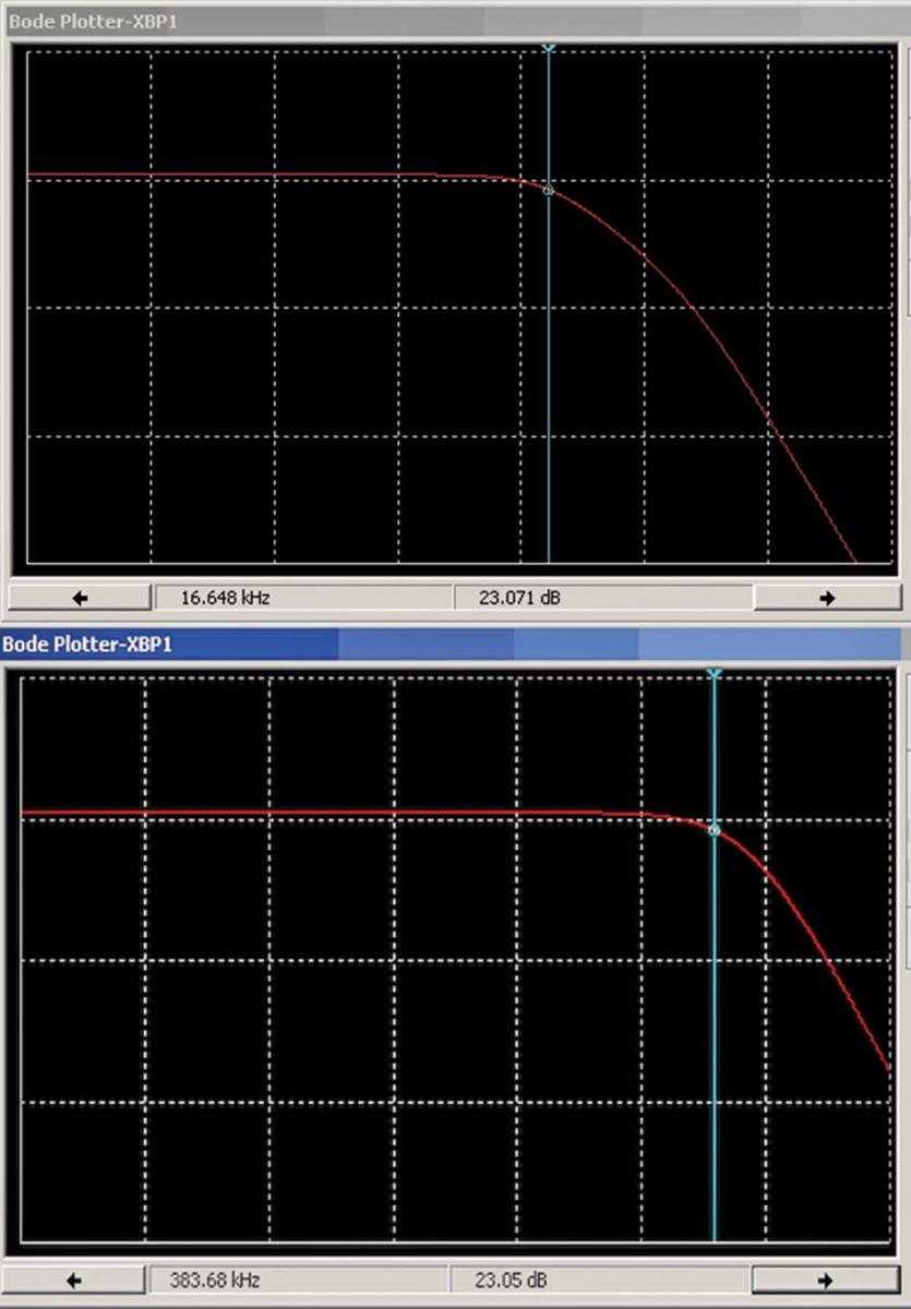
| Figure 2. | Spice plots demonstrate the improvement in circuit bandwidth offered by JFET bootstrapping. Without the bootstrapping, the circuit bandwidth is 16.6 kHz. With the bootstrapping JFET, the bandwidth increases to 383.7 kHz. |
|
Bootstrapping Benefits
The bootstrapping scheme also has beneficial effects on noise. The noise of a photodiode amplifier operated as a transimpedance amplifier (TIA) is a complex combination of diode noise, amplifier current noise, amplifier voltage noise, and the Johnson thermal noise of the feedback resistor. The amplifier's offset voltage and input equivalent voltage noise is multiplied by noise gain of the circuit and appears at the output. Analog Devices’ op-amp handbook [2] demonstrates that the dc noise gain is
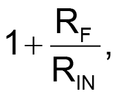
and the ac noise gain is
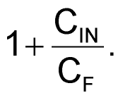
Since the bootstrapping makes the diode resistance look infinite, the dc noise gain is 1. That means the amplifier's offset voltage isn’t multiplied when it appears at the output.
The ac condition is almost as good. Without the JFET, the input capacitance is the diode capacitance plus the amplifier input capacitance plus any stray capacitance on your printed-circuit-board (PCB) layout. The 3000-pF diode capacitance dominates this, so that the ac noise gain is 1 + 3015/0.25 or 12,061. With the JFET, the circuit input capacitance drops to the sum of the JFET capacitance, the amplifier input capacitance, and the stray capacitance.
Now the ac noise gain is 1+25/0.25, or 101. The amplifier's equivalent input noise is multiplied by this ac noise gain. The improvements in the circuit's noise performance are obvious when the ac noise gain goes from 12,061 to 101. The 1-nV/√Hz contribution of the JFET adds RMS to the amplifier noise of 8 nV/√Hz, to give 8.2 nV/√Hz. The RMS addition means the much larger amplifier input equivalent noise is dominant.
Unfortunately, the JFET does put a dc voltage across the photodiode. You can infer this by drawing the load line of the JFET 4990-Ω resistance on the JFET transfer curves as published in its datasheet (Fig. 3). Since the plus pin of the op amp is at ground, the minus pin must also be at ground, if you ignore any offset voltage error. That means the JFET gate is at ground. So, when the gate-source voltage goes from –1 to 0 V, the voltage across resistor RBIAS goes from 6 to 5 V. Therefore, the current through RBIAS and the JFET goes from 1.2 mA to 1 mA.
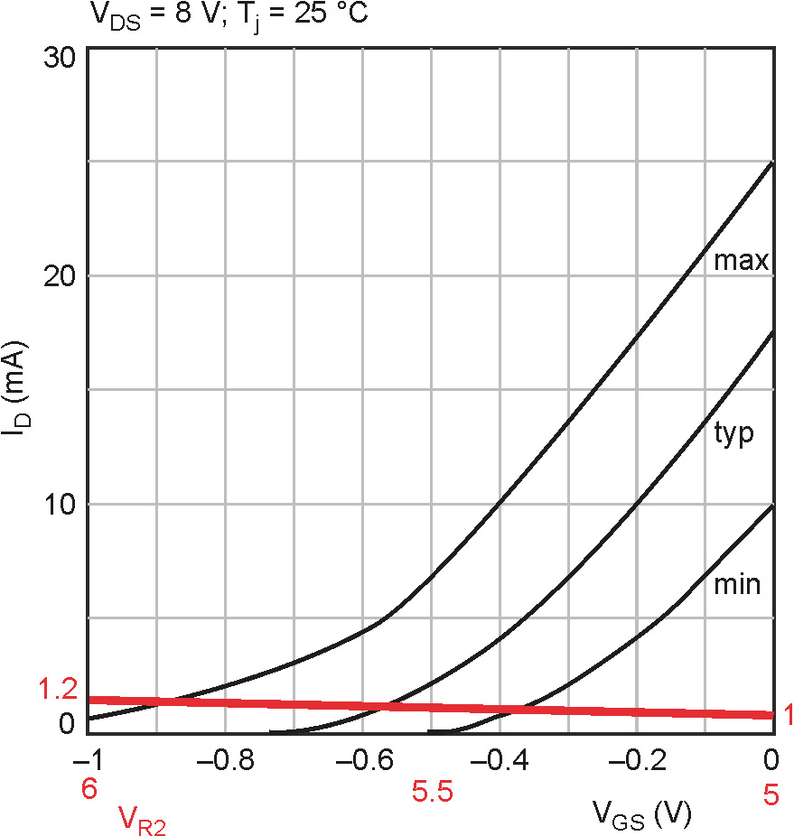 |
||
| Figure 3. | Drawing the 4.99-kΩ load line on the transfer curves from the JFET datasheet shows the 0.35- to 0.9-V dc error that will appear across the diode with different JFETs. |
|
Drawing that load line on Figure 3 of the BF862 datasheet shows a 0.35- to 0.9-V reverse bias across the diode that will create a dark current flow in the photodiode. This dc current will appear at the output as an error. Worse yet, this error will be different in every circuit as you use JFETs with minimum, maximum, and typical JFET transfer characteristics. The dc voltage and the error it creates will also change with temperature.
Make the Move to Matched
Kirkwood Rough of Upstairs Amps suggested using a matched dual-JFET. This removes the bulk of the dc voltage across the photodiode (Fig. 4). The lower JFET replaces the resistor with a current source, which improves the response of the voltage follower and makes it more accurate.
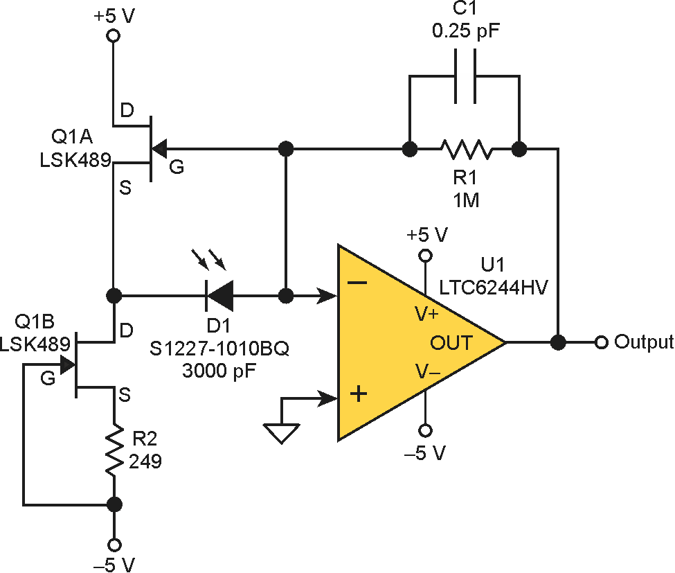 |
||
| Figure 4. | Using a dual-JFET improves the bootstrapping and reduces the dc voltage across the diode. The capacitance across the source resistor reduces the resistor noise contribution. |
|
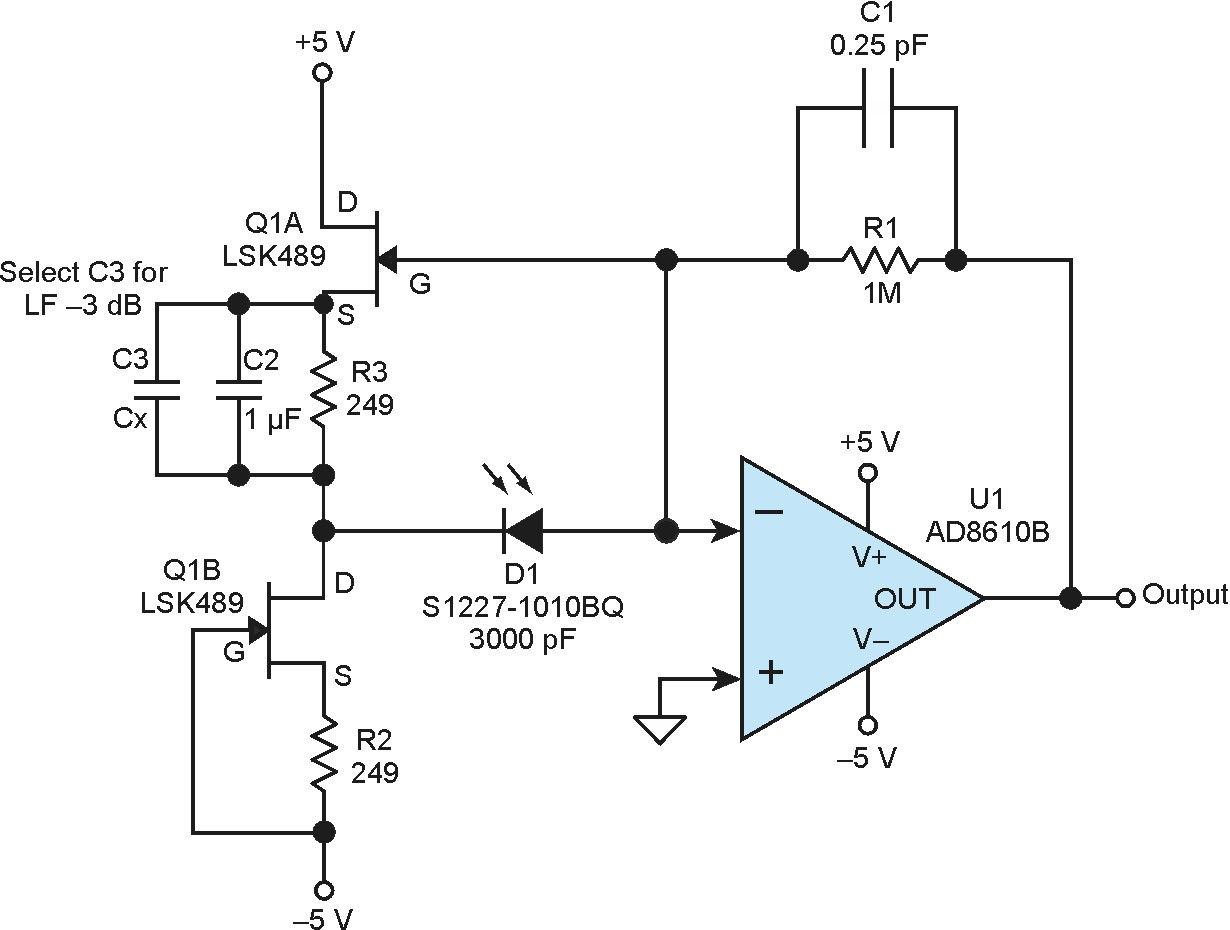
Scott Wurcer, a Fellow at Analog Devices, suggested that matching the source resistors of the JFETs ensures that the cathode of the photodiode will be very close to 0 V (Fig. 5). Using an amplifier with lower offset voltage also minimizes any dc across the diode. You can add a capacitor across the bootstrap JFET source resistor to reduce the noise contribution of this added resistor.
 |
||
| Figure 5. | The dc offset across the photodiode is further reduced by matching the source resistors of the two JFETs. | |
The LSK489 dual-JFET has superior transconductance to the BF862. That, combined with the current-source load presented by the other JFET, improves the bootstrapping, especially at higher frequencies. The AD8610B amplifier has 2-nv/√Hz lower voltage noise, which will further reduce ac noise. It has one-seventh bias current, which will reduce the dc output error. It also has half the offset error of the LTC6244.
Nothing is for free, though – the AD8610B has half the bandwidth and will cost you at least a dollar more. Not only that, it’s a single whereas the LTC6244HV is a dual. For this circuit, the bandwidth should be adequate, but cost is always a concern.
 |
||
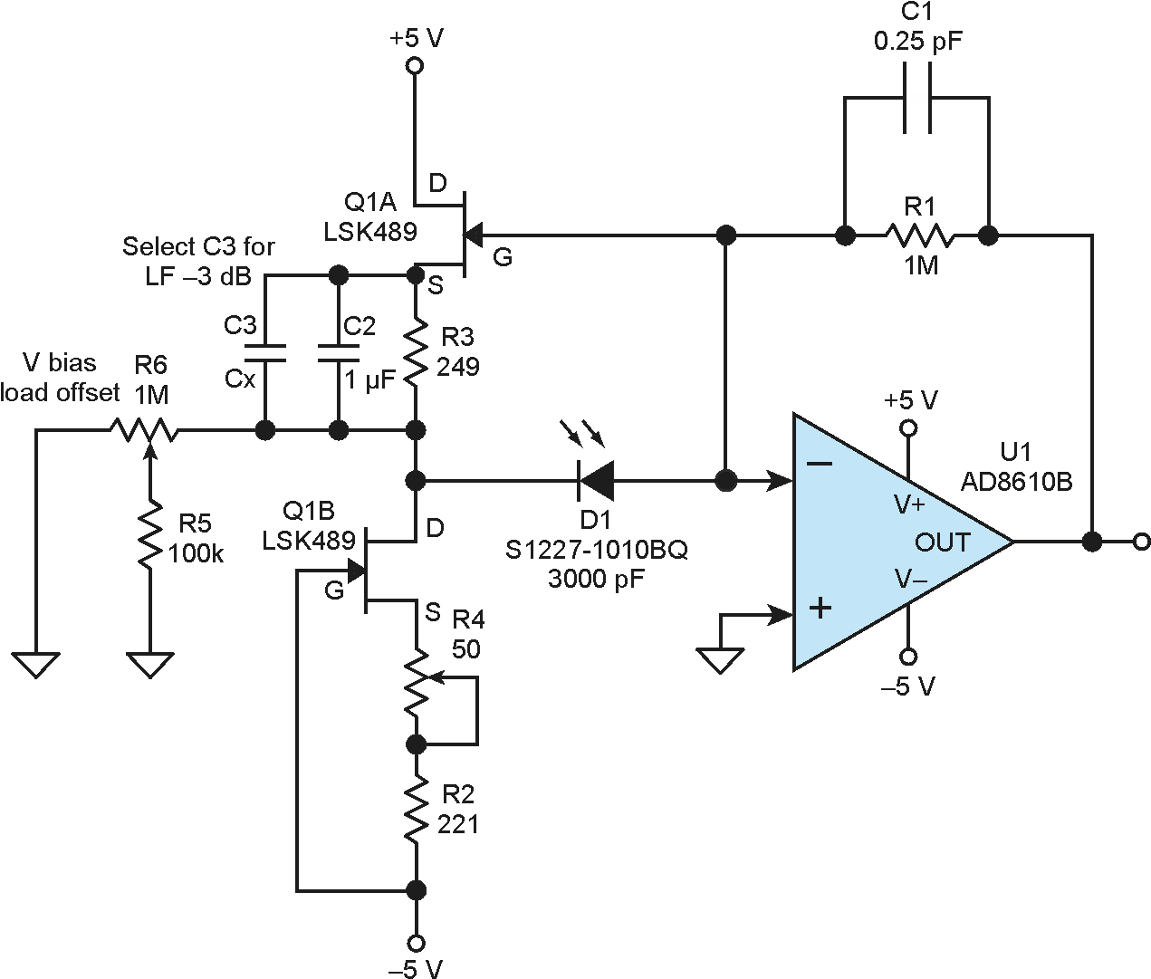
| Figure 6. | By using potentiometers, you can tweak out any tiny offset voltage across the photodiode. This completely eliminates any dark-current error. |
|
The proposed circuit will still have variable, albeit small, dc errors due to resistor tolerances. To bring the voltage at the cathode of the photodiode to within a few microvolts of ground, you can add adjustment potentiometers to the circuit (Fig. 6), another Kirkwood Rough suggestion. Wurcer [3] suggested a low-offset op amp could servo the bias point to a few microvolts. Paul Grohe of Texas Instruments pointed out that even laboratory power supplies add a lot of noise to our circuits [4].
To get the optimum noise measurement, you should power these circuits with batteries. You can then use that as a baseline to evaluate the noise contribution of the power supplies in your production design.