The growth of battery-operated applications has put steady pressure on designers to steeply reduce their products’ operational power consumption and bring standby power as close to zero as possible by carefully managing the devices’ quiescent currents. In this Design Idea, we’ve taught the classic 555 timer IC (Ref. 1) to consume zero current in its quiescent mode and wake up quickly in a known state. It is a pleasure to find an innovative way to use this classic device (Fig. 1) because we have a long history together. In fact, I still remember the thrill of playing with 555 timer ICs during a long summer break from school at the age of 15. By way of thanks for those memories, I dedicate this article to Hans Camenzind (Ref. 2) for his invention of this great little chip.
 |
||
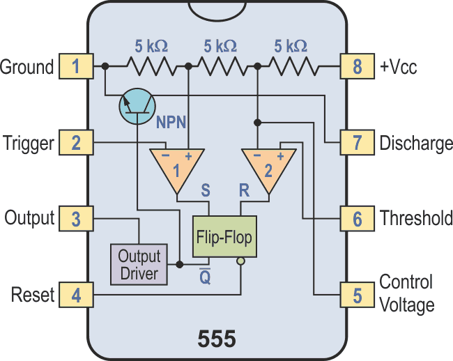
| Figure 1. | This simplified block diagram represents the internal circuitry of the 555 timer. |
|
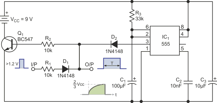
The highlights of this design (Fig. 2) are that it is versatile and easily adaptable, uses off-the-shelf components, has a low component count, is activated by a positive going trigger input, and draws zero off current.
 |
||
| Figure 2. | This diagram shows a 555 timer circuit with zero quiescent current. | |
Monostable operation
In this mode of operation, the timer functions as a one-shot. The circuit operates in the following manner. A short pulse (> 1.2 V) applied to point I/P energizes transistor Q1, pulling the 9 V battery’s negative terminal down very close to the circuit’s GND value. The resulting pulse triggers an immediate output from pin 3 of the 555 IC, which holds the transistor Q1 ON for the duration of the time delay determined by the values of R3 and C1.
When the voltage across the capacitor C1 equals 2/3 VCC, the comparator resets the timer’s internal flip-flop, driving its output (pin 3) to a low state, thereby turning off the transistor Q1. Once Q1 is turned off, it is no longer in pull-down mode, so the whole circuit is now drawing zero quiescent current.
Timing adjustments
The 555’s output pulse width can be lengthened or shortened to the meet your application’s requirements by adjusting the values of R3 and C1. The output pulse width of time T is given by
T = 1.1×R3×C1.
Usually a 555 timer IC is limited because it requires a negative going trigger input but in this design, it is triggered on a positive going pulse which takes the IC out of its zero-current quiescent state for the duration of its programmed time cycle.