Light sensors find use in a host of important applications, spanning from consumer electronics, such as ambient-light measurements and exposure control for cameras, to scientific instruments, such as optical-absorption spectroscopy, IR (infrared) detection for thermography, and two-color pyrometry. For example, in optical spectroscopy, a correct intensity measurement of the probe beam is fundamental during material and device characterization. You must eliminate any influence that dc or very-low-frequency background light induces. Also, to increase the SNR (signal-to-noise ratio), you can apply narrowband, phase-sensitive, or lock-in detection techniques to mechanically chopped or otherwise modulated probe-light sources.
 |
||
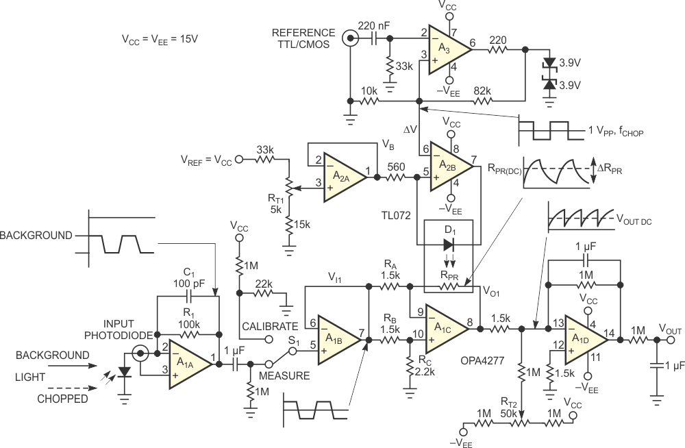
| Figure 1. | The reference signal from a light chopper acts as a square wave of frequency and modulates the gain of an op-amp- based inverting amplifier. |
|
In this Design Idea, the reference signal from the light chopper as a square wave of frequency, fCHOP, modulates the gain of an op-amp-based inverting amplifier (Figure 1). The amplifier input is a voltage proportional to the photocurrent signal produced by a photodiode, which is irradiated by a modulated light beam at the same chopper frequency. In this case, because the gain and input are at the same frequency content, a dc component, which a lowpass filter can easily detect, is present at the amplifier’s output.
Op amps A1A and A1B convert the photogenerated current into a voltage including only the ac components. You can change the value of R1 depending on the light level you want to detect. Neglecting A1A’s input capacitance, the value of C1 strongly depends on the terminal capacitance of the input photodiode, and you must select the value to ensure the stability of the transimpedance circuit (Reference 1).
The heart of the system, op amp A1C, includes photoresistor RPR, which represents the feedback element that determines the gain of the stage. The value of RPR depends on the light that D1 emits. A2B, a voltage-to-current converter, drives D1. The converter has a fixed voltage, VB, and a ΔV signal through A2A and A3. A2A determines the dc value of RPR, whereas A2B and ΔRPR change at the same frequency as the reference signal. The A3 Schmitt trigger converts any TTL/CMOS level of the reference signal into a balanced ±4.6 V square wave attenuated to ±0.5 V to generate an LED current change of approximately 1.8 mA p-p. For the photoresistor, RPR, and LED elements, a LUNA optoelectronics CdS (cadmium-sulfide) NSL-19M51 cell couples to a red LED and resides in a black box to ensure the absence of background light on the optocoupler.
To calibrate the circuit, first disconnect or obscure the input photodiode so that A1A converts no ac signal. Then, switch S1 to the “measure” position and adjust RT2 to null any voltage offset referred to the output voltage. When the A1B buffer generates the known approximately 300-mV test voltage and S1 is in the calibrate position, adjust RT1 to fix the output voltage at 0 V. In such a case, VB voltage can set the RPR/RC = RA/RB condition.