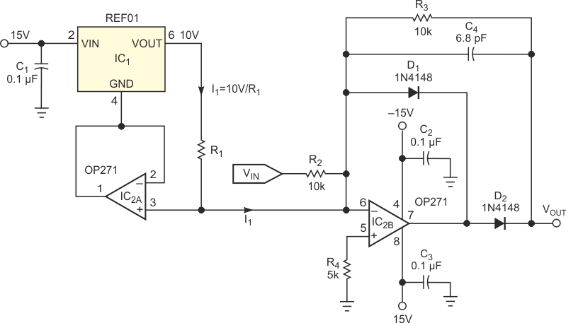
Deadband circuits find applications in servo-control systems. A precision current source and a half-wave inverting rectifier form a positive deadband circuit (Figure 1). The REF01, IC1, is a precision 10 V voltage reference. It forms a precision current source with the addition of a unity-gain buffer (IC2A) and resistor R1. IC2A forces the ground pin (Pin 4) of IC1 to assume the potential at IC2A 's noninverting input. IC1 forces its highly accurate reference voltage (10 V) across R1, so the current I1 through R1 is 10 V/R1. Because the inverting input of IC2B connects to the output of the current source, the feedback diode, D1, becomes forward-biased with current I1. The forward-biased diode keeps the output of IC2B at approximately –0.6 V. Because the cathode end of D2 stays at virtual ground through R3, D2 remains reverse-biased. Hence, VOUT remains at virtual ground (0 V). Any positive voltage applied to VIN further forward- and reverse-biases D1 and D2, respectively, and the output remains at 0 V (deadband zone) for VIN > 0 V.
 |
||
| Figure 1. | This circuit exhibits a deadband for signals more positive than an arbitrary voltage, which R1 determines. |
|
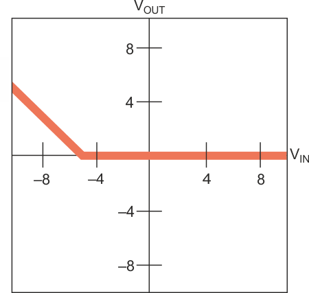
Negative inputs tend to forward-bias D2 and reverse-bias D1. This bias situation occurs only when the current through R2 (because of the negative VIN) equals or exceeds 10V/R1. So, the output is 0 V (deadband) until VIN reaches a value equal to –10R2/R1. If you choose R1 = 20 kΩ, VOUT remains at 0 V for VIN > (–5 V); for VIN ≤ (–5 V), VOUT = (–VIN –5 V). Figure 2 shows the transfer function for this scenario. C1, C2, and C3 are decoupling capacitors for IC1 and IC2. R4 reduces the offset voltage of IC2B in the nondeadband region. You could realize an alternative straightforward circuit by prebiasing the inverting half-wave rectifier through a precision resistor connected to a voltage reference without using the unity-gain buffer, IC2A. However, this alternative would increase the noise gain, thereby increasing the offset and noise at the output.
 |
||
| Figure 2. | With R1 = 20 kΩ, the circuit in Figure 1 is “dead” for input voltages higher than –5 V. |
|