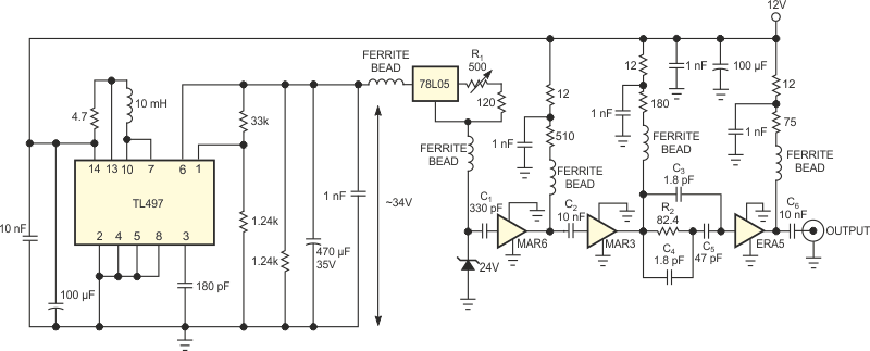
A broadband source of white noise can be useful for measuring and testing communications equipment. The source in Figure 1 is simple and produces a large noise signal at its output terminals. The circuit comprises a zener diode and a few amplifying stages. The breakdown occurring in the zener diode is the true source of broadband noise in this design. This process is truly broadband because a substantial amount of noise is measurable at frequencies higher than 2 GHz.
 |
||
| Figure 1. | A 24 V zener diode and a series of MMIC amplifiers create a broadband noise source. | |
The circuit ac-couples the zener diode into the first amplifier stage, and subsequent stages build up the zener diode's tiny noise voltage. The amplifiers-the MAR-6, MAR-3, and ERA-5 (Mini-Circuits) are monolithic-microwave ICs (MMICs). The total voltage gain of approximately 58 dB is high enough to produce an output voltage of approximately 224 mV rms at the 50 Ω terminating load, which is equivalent to approximately 0 dBm. Each amplifier in the chain has a compression point 1 dB higher than that of the previous amplifier. Good amplifier linearity is important to ensure that the output signal has a Gaussian probability-density function. The 1-dB compression point for the last amplifier in the chain is more than 18 dBm to ensure that the amplifier operates in the linear mode.
From observations and measurements, it appears that the noise level of the avalanche-type breakdown diodes prevails over the noise based on the tunnel effect, and this noise level increases with the zener voltage of the diode. The frequency spectrum of the noise signal is independent of the zener diode's voltage value, although a higher breakdown voltage typically means lower bandwidth. Using a zener diode with a 24 V breakdown voltage for the circuit in Figure 1 allows the design to produce a 10-dB-greater output signal than a design that uses a 9.1 V zener diode.
 |
||
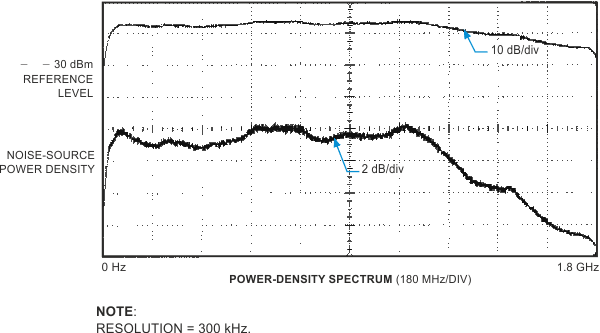
| Figure 2. | A power-density spectrum of the noise source shows a flat spectrum with an accuracy of ±1 dB from 20 MHz to 1 GHz. |
|
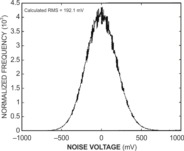
A switching regulator, the TL497, and associated components provide the supply voltage for the zener diode; a 12 V source supplies power for the rest of the circuitry. An additional linear regulator, the 78L05, supplies current to the zener diode. Changing the value of the current through the zener diode by trimming R1 allows you to obtain a flat frequency spectrum from the source. You can increase the current to some value to find an optimum point for which the noise spectrum is flat and the noise level is as high as possible. For this design, the optimum current is approximately 21 mA. Increasing the current beyond this optimum point is not recommended because further increases cause a decrease of the output signal. Figure 2 is a plot of the noise-power-density spectrum, measured with a spectrum analyzer. In the frequency range of 20 MHz to approximately 1 GHz, the spectrum is flat with an accuracy of ±1 dB, and the 3-dB bandwidth is approximately 10 MHz to 1.35 GHz. The probability-density function measured for 107 samples has the well-known Gaussian shape (Figure 3). The calculated rms value from the histogram differs slightly from the power-measurement value; this difference stems from the limited bandwidth of the sampling gate used to acquire the samples.
 |
||
| Figure 3. | The probability-density function has a Gaussian shape, and the calculated rms value is 192.1 mV. |
|
To achieve a flat power-density spectrum of the noise in the low-frequency region, some spectrum whitening is necessary because of the existence of 1/f-type noise. This circuit achieves the necessary frequency shape of the amplifier gain using properly chosen values of coupling capacitors between amplifier stages-C1, C2, and C6 -and by using a correcting network before the last stage-C3, C4, C5, and R2. The values of all frequency-shaping components were chosen experimentally while observing the power-density spectrum on the analyzer screen.
To obtain good performance from the circuit, you must obey all RF design rules. In particular, keep the pins of the zener diode as short as possible and locate all decoupling capacitors near the MMIC amplifiers. Screening the entire circuit is also recommended.