Sawtooth- or exponential-ramp relaxation oscillators are common and generally easy to build. However sometimes a cleaner waveform is desired, and generators of even-symmetric waveforms are a bit more difficult to design.
Triangle wave generators are typically implemented using an op amp integrator and comparator; see for example references [2] and [3]. It takes some effort, however, to devise an op amp triangle wave circuit which also provides voltage-controlled frequency.
This Design Idea presents a voltage-controlled triangle wave generator with a good-quality waveform, reasonably wide frequency range, and a small number of components. It is not much more complex than a sawtooth relaxation oscillator, and uses a single capacitor.
Good results are obtained with components of common tolerances and no deliberate matching.
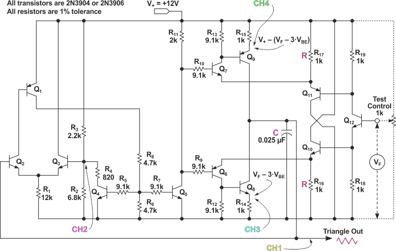
The circuit is shown in Figure 1. The frequency of the signal available at Triangle Out is a linear function, detailed below, of the input voltage VF. The bold-faced R and C are primary frequency-determining components.
 |
|
| Figure 1. | Schematic for the voltage-controlled triangle wave generator. |
To get wide range, a high-impedance amplifier is required, to allow small currents to charge a capacitor to the required threshold level. This amplifier is the differential amp formed by Q2 and Q3. A 12 kΩ emitter bias resistor implies an impedance at the base of Q2 in the 1-megohm range.
At power-on, the voltage at the base of Q2 is zero, and at the base of Q3 about 9 V. Thus Q3 is on and Q1, Q2, Q4, and Q5 are off. This causes Q7 to turn on, which activates current source Q9, so the voltage on C begins to ramp up, linearly.
Upon reaching the threshold voltage (6 V), Q2 begins to conduct and hence so does Q1, connected here as a high-gain stage. Q1 in turn causes Q4 to conduct, pulling the threshold voltage down further. This positive feedback loop boosts the switching speed. Since there is delay induced by Q5 and Q7/Q9 or Q6/Q8, C continues to charge and we are therefore assured that switching will complete. At this point the voltage at the base of Q2 is a little over 6 V, and the threshold voltage, at the base of Q3, is at about 3 V. Current source Q8 is switched on, and drains current from C at the same rate that Q9 charged it. When the ramp gets below the threshold voltage, the cycle repeats.
The current sources driving C are fed by a given voltage VF (minus a VBE) and its complement, as developed on the emitter and collector of Q12, respectively. Q11 lowers the output impedance of the collector output from Q12. Q10 balances out Q11 by introducing a corresponding VBE drop. The voltage across R17 is therefore equal to the voltage across R16.
Since Q6 and Q7 run as complementary switches, controlled by switching transistor Q5, they are driven to saturation, and this will sink base current from the corresponding emitter of Q10 or Q11. However these base currents are still quite low as compared to the current through R, and are also the same for each side. So symmetry of the triangle wave is maintained.
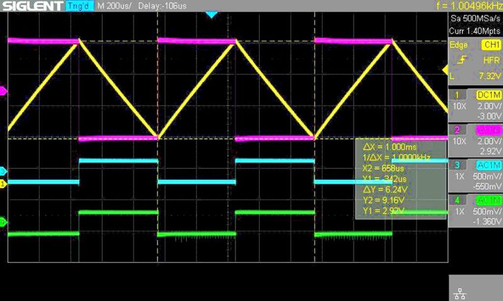
Since the output is taken directly from the capacitor C, it subsequently should be buffered by a high-impedance amplifier. The scope trace in Figure 2 shows waveforms as indicated by the channel indicators CHn in the schematic. Note that all channels except channel 1 are AC coupled.
The frequency of oscillation may be determined by calculating the charging time of C from the current sources, between the limits of the high and low thresholds VTH and VTL; double this number gives the period. The frequency F so derived is a linear function of VF and is given as follows:
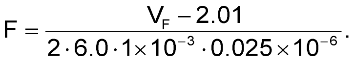
With component values as shown in the schematic, VTH = 9 V, VTL = 3 V, and VBE = 0.68 V:
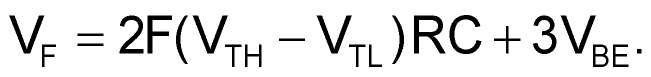
At a measured VF of 2.36 V, F = 1066.67 Hz. This matches the measurement of 1004.96 Hz shown in the scope trace fairly well. The input voltage needed to produce a given frequency is given by:
In the particular case here:

The rate of frequency change is about 3 kHz/V, or 3 Hz/mV; the control is thus fairly sensitive. At a frequency of 2 kHz, the calculation gives VF = 2.64 V, and at 4 kHz, VF = 3.24 V. Measuring VF at these frequencies produces 2.71 V and 3.46 V, respectively, which comport reasonably with the calculated values, especially considering the sensitivity. Good triangle symmetry is retained up to just over 6 kHz and down to about 600 Hz.
Oscillation will cease when the voltage on the emitter of Q8 exceeds the lower threshold voltage VTL. In this case this is at about 3 V, or an input voltage VF of about 5 V. At the low end, a VF of a bit over 2 V is needed to overcome the three base-emitter drops in the path.
 |
|
| Figure 2. | Scope trace, measurement points as shown in the schematic. |
The square wave shown in channel 2 of the scope trace of Figure 2 is obtained from the base of Q3, i.e., the threshold input to the differential amplifier. Note that the fall time is significantly less than the rise time. This is due to the fact that the positive feedback loop which operates on the upswing is not effective on the downswing, so Q4 and Q5 turn off more slowly than they turn on. This only minimally affects the triangle wave, since the turn-on threshold for Q7 is quite low, thereby assuring the triangle slope is reversed in a timely manner.
 |
|
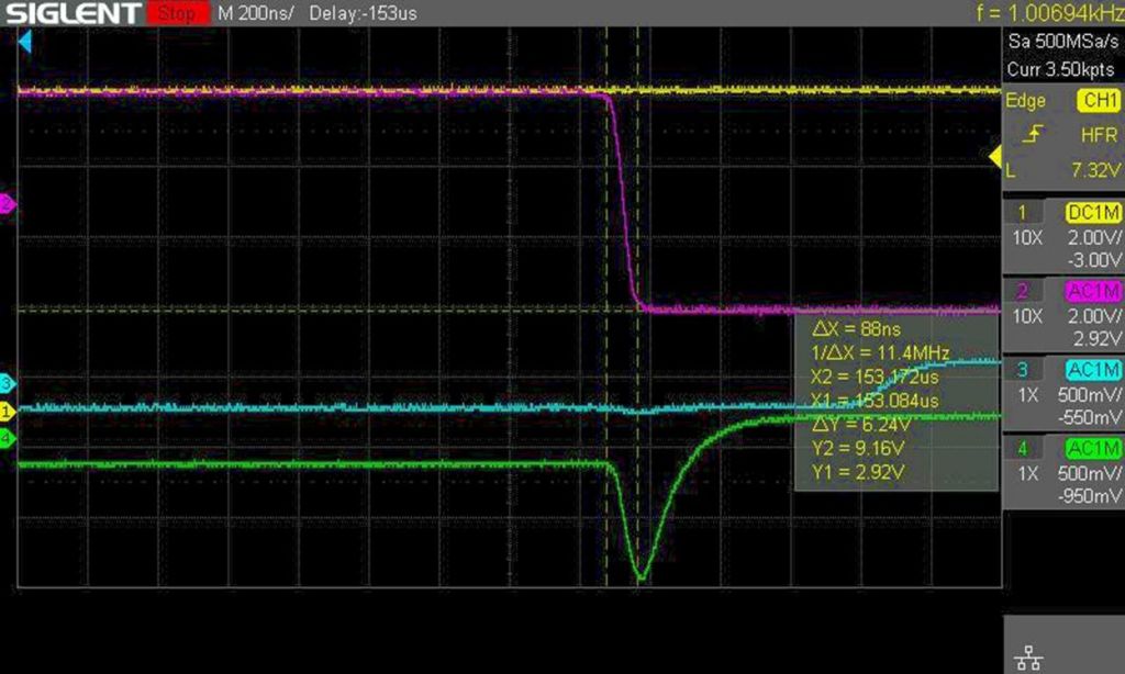
| Figure 3. | Fall time. |
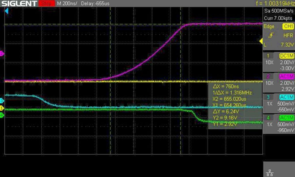
The scope traces shown in Figure 3 and Figure 4 display this disparity. In Figure 3 the fall time is about 88 ns while the rise time, shown in Figure 4, is 760 ns. Note, though, that channels 3 and 4 in these traces show the rise and fall times on the emitter resistors of the current sources (Q8 and Q9), and that they remain low, in the 75 ns range. However, there is switchover delay, about 600 ns in one case and about 1.6 μs in the other.
 |
|
| Figure 4. | Rise time. |
All of the resistors used are 1% commodity parts that can be obtained readily and inexpensively. The transistors as well are from a commercial batch and have not been matched or otherwise selected. There are several basic variations on the circuit that may be interesting to pursue. A wider frequency range may be supported by lowering the Δ-Threshold. More amplification could of course then be required. Control over duty cycle could also be added. Finding values of R and C that optimize power, range, or resolution may also be worthy of pursuit. The values chosen here are somewhat arbitrary – but not capricious: for example, I ran out of 10 kΩ resistors, so I used 9.1 kΩ instead.
An interesting challenge is to design a more symmetrical circuit. This might, for example, provide positive feedback on crossing both the high and low thresholds, addressing the rise/fall time issue, and potentially expanding the frequency range.