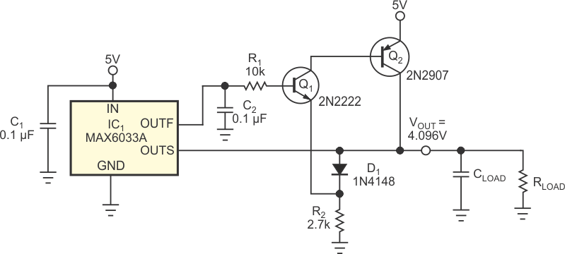
Large analog systems that present many loads to a voltage-reference source can often demand more current than a single reference IC can deliver. However, if the reference IC includes force and sense terminals, you can easily add a buffer to the circuit's feedback loop without affecting the reference's accuracy. For example, the circuit in Figure 1 provides the same 0.04% initial accuracy and 7-ppm/°C temperature coefficient as IC1, a stand-alone MAX6033. The buffer circuit delivers as much as 80 mA.
 |
|
| Figure 1. | Add a two-transistor output buffer to a 4.096 V, 15-mA reference IC to boost its output current to 80 mA or higher. |
When you design a buffer stage for a force/sense-control loop, the buffer must provide unity-voltage gain with no phase inversion. In addition, the circuit's power supply must provide head-room voltage to accommodate the reference voltage plus voltage drop across the buffer stage. The simplest buffer circuit comprises an NPN transistor that connects as an emitter follower, which requires a drive voltage that exceeds the reference's output voltage by one transistor base-emitter voltage drop. If you add the required minimum power-supply voltage plus the maximum allowable base-emitter voltage, the configuration runs out of head room. Using a PNP stage to drive the emitter drive stage solves the head-room problem but inverts the output voltage and prevents the force/sense loop from functioning. Adding a second PNP stage cancels the phase inversion but destabilizes the force/sense loop by adding excessive gain.
The modified complementary Darlington, or Sziklai, connection (Reference 1) in Figure 1 solves both problems by providing an emitter follower's unity-voltage gain with no inversion. The output PNP stage provides plenty of head room, but the NPN stage does not. You can easily overcome this drawback by adding diode D1 to shift the NPN transistor's emitter voltage downward by a diode drop. Thus, to a first approximation, the diode's voltage drop and the transistor's base-emitter voltage cancel one another, leaving plenty of voltage head room. Transistor Q2, a 2N2907, provides limited current gain, which in turn limits the circuit's maximum output current to 80 mA. Substituting a higher gain transistor can increase the output current to any reasonable level.
For stability, the MAX6033 requires 0.1-µF ceramic bypass capacitors on its IN and OUTF pins. Capacitor C2 determines the circuit's response speed, but the buffer circuit exerts no significant effect on transient response. Most dc-reference-voltage ICs cannot accommodate a fast-changing load-current step; thus, the circuit's transient response and its ability to supply fast current spikes depend on the output capacitor, CLOAD. Values of CLOAD as high as 10 µF do not affect the circuit's stability.