Experimenting with an HF oscillator, I needed to control the varactor diode voltage in precise increments over a 2 V-10 V range. A buffered potentiometer was the obvious choice, and connecting two pots in series to give coarse/fine control (or using a multiturn pot) would offer improved control over the varactor voltage. However, this approach still didn't allow me to generate uniform increments and decrements of the control voltage in a reliable, repeatable manner. I needed a solution that would provide the necessary precision together with complete flexibility over the size of the voltage increments.
I eschewed a microcontroller-DAC arrangement as this would require specialized components and the voltage increments would be dependent on the DAC resolution (and I was too lazy to write the code anyway). A digipot with up-down control was another possibility: this would offer a non-volatile solution like the DAC approach, but again, the increments would be entirely dependent on the pot's resolution.
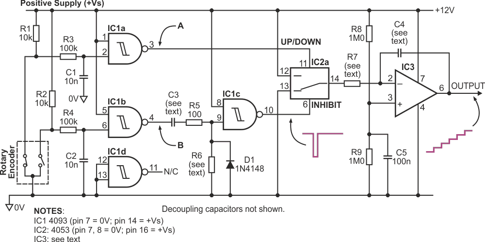
The solution documented in this Design Idea can be assembled using inexpensive, readily available components, and the voltage increments are user-definable (Figure 1). An inexpensive rotary encoder is used to control the output voltage – a single step of the encoder increments or decrements the voltage by a precise amount, providing easy up/down control like a conventional pot.
 |
|
| Figure 1. | The rotary encoder controls a staircase waveform with precisely defined steps. |
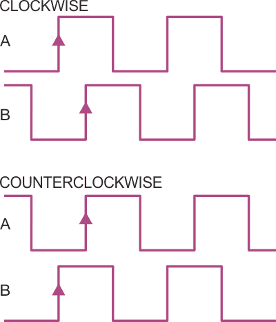
The outputs of an incremental encoder typically consist of two signals in quadrature (i.e., phase-shifted by a quarter period), which produce a specified number of pulses per shaft revolution, each pulse corresponding to an increment of rotation. Internally, the encoder has two switches connected to a common terminal. This terminal is usually connected to ground, and the two outputs are connected to pull-up resistors (R1, R2). R3/C1 and R4/C2 provide contact debouncing, with IC1a and IC1b producing squared-up signals at points A and B. The encoder should be connected so that when it is rotated clockwise, the rising edge of signal A leads the rising edge of signal B by a quarter period; conversely, when it turns counterclockwise, signal B leads A by a quarter period (Figure 2).
 |
|
| Figure 2. | Rotary encoder outputs. |
C3, R6, and IC1c implement a conventional digital differentiator or monostable which generates a narrow, negative-going pulse whose width is dependent on the C3-R6 time constant. This pulse is generated on the rising edge of signal B and is used to enable analog switch IC2a by means of the INHIBIT input. Whenever this input is high, the analog switch is completely open-circuit and no current flows through integrator resistor R7. When the output of IC1c pulses low, the switch closes, and R7 is momentarily connected to either the positive supply rail or ground, depending on the UP/DOWN input. The state of the UP/DOWN signal when the analog switch is enabled depends on the rotation direction of the encoder.
If the encoder is rotated CW, signal A will be high when the INHIBIT pin is pulsed, connecting R7 to ground and depositing a discrete packet of charge into C4, which increases the output by one step size. This is of course reversed for CCW rotation. In this manner, each click of the encoder moves charge into or out of C4 as determined by the brief pulse of current through R7.
As described above, each packet of charge is integrated by C4 & IC3. To understand how this section behaves, assume that C4 is initially uncharged. The voltage set by R8 & R9 at the op-amp's non-inverting input is equal to +Vs/2 (6 V in this example), and closed loop feedback around the op-amp will maintain the inverting input at the same level. This means that the right-hand terminal of R7 always sits at +Vs/2. Since there is no voltage across C4, the op-amp's output will also initially be at +Vs/2.
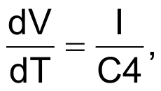
When the analog switch closes, the left-hand terminal of R7 is connected either to 0 V or to +Vs. Ignoring op-amp bias current and analog-switch resistance, the magnitude of the current pulse into the integrator is given by:
For example, with a supply of 12 V and R7 = 100 kΩ, the pulse magnitude would be 60 µA.
If the encoder is rotated in a clockwise direction, the UP/DOWN signal is high during IC1c's output pulse, connecting R7 to 0 V and sinking charge out of C4. Therefore, in order to maintain overall equilibrium by keeping the inverting input at +Vs/2, the op-amp must dump charge into C4, which results in a single increment of the output voltage. On the other hand, if the encoder is rotated counterclockwise, the UP/DOWN signal is low, causing R7 to be connected to +Vs and sourcing charge into C4. Consequently, the op-amp must suck charge out of C4, which results in a single decrement of the output voltage.
The resulting output forms a staircase of equal-amplitude steps which moves upwards or downwards depending on the rotation of the encoder. The step magnitude is determined by the width of the pulse at the INHIBIT input, and by the values of R7 and C4. Now, from first principles, we know that:
and
Rearranging and simplifying these equations allows us to determine the magnitude of the output steps:
where I is the magnitude of the current pulse through R7, dt is the duration of the pulse output by IC1c, and C is the value of C4.
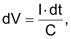
With fixed values of C3 and R6, dt will be a constant, and if +Vs is held constant, the value of I will be determined only by R7 (assuming that the analog switch on-resistance is insignificant). Consequently, dV can be varied to suit your requirements via the R7 and C4 values. For example: C3 and R6 are chosen to make dt = 100 µs, and C4 = 100 nF. With R7 of 100 kΩ – resulting in pulse current I = 60 µA – we find that the nominal step size dV is 60 mV. In a test circuit built with C3 = 1 nF and R6 = 100 kΩ (giving dt ≈ 100 µs), the actual step size was measured as 59.7 mV (Figures 3a and 3b).
 |
|
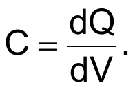
| Figure 3a. | Output waveform created by CW and CCW encoder rotation (4s/div., 2V/div.). |
 |
|
| Figure 3b. | Expanded view of output waveform shows individual increments. |
The circuit powers up with the output at mid-rail voltage. The output voltage tends to drift over time. Voltage drift can be estimated from:
where I is the total leakage current. The leakage current is a combination of the op-amp's input bias current at the inverting input plus the off-state leakage current of the analog switch. Clearly, the voltage drift can be minimised by choosing a large value for C4 and by keeping leakage currents as low as possible. In this respect, CMOS or JFET op-amps are best since they have extremely low input bias currents – usually in the picoamp range. The off-state leakage current of the 4053 analog switch is typically around 50 pA at room temperature, although it can be as high as 100 nA for some types. This can be minimised by replacing the standard 4053 with an improved version such as the MAX4053A, which has a maximum leakage current of just 100 pA at 25 °C. It also has lower on-state resistance than the standard 4053.
The voltage drift tends to be worse at the extremes of the output voltage range, where the voltage across C4 is largest. In the test circuit built using a conventional 4053 and an LMC6081 CMOS op-amp, the average drift was 6.8 µV per second.
For a given supply voltage, the output voltage range is dictated by the type of op-amp used. If you need the output to swing from 0 V to +Vs, you'll need an op-amp with rail-to-rail output capability. The TLC271 is a good choice, although the LMC6081 provides better guaranteed output swing. Both of these devices have extremely low input bias currents. Note that the op-amp doesn't need to have rail-to-rail input capability since both inputs are held at mid-rail voltage at all times.
Although the integrator circuit has a degree of inherent noise rejection, careful layout and decoupling is still essential to prevent digital noise from coupling into the output signal. R8 and R9 should be well matched to ensure that the output voltage increment and decrement steps are of equal value. The test circuit's quiescent supply current was just 0.5 mA, rising to around 1.5 mA when the encoder was rotated.
 |
|
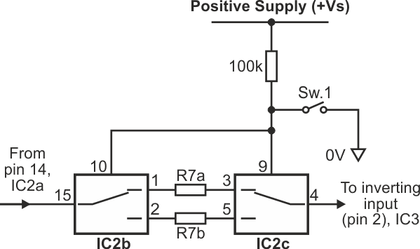
| Figure 4. | Circuit enhancement allows for fine and coarse control over output step size. |
Figure 4 shows how the design can be enhanced to provide fine and coarse control over the output steps. This additional circuit makes use of the unused switches in IC2. Here, the integrator resistor R7 has been split into two different parts: R7a and R7b. With switch Sw.1 open, the analog switches are in the positions shown, and the integrator current is set by R7a. With the switch closed, the analog switches select R7b.