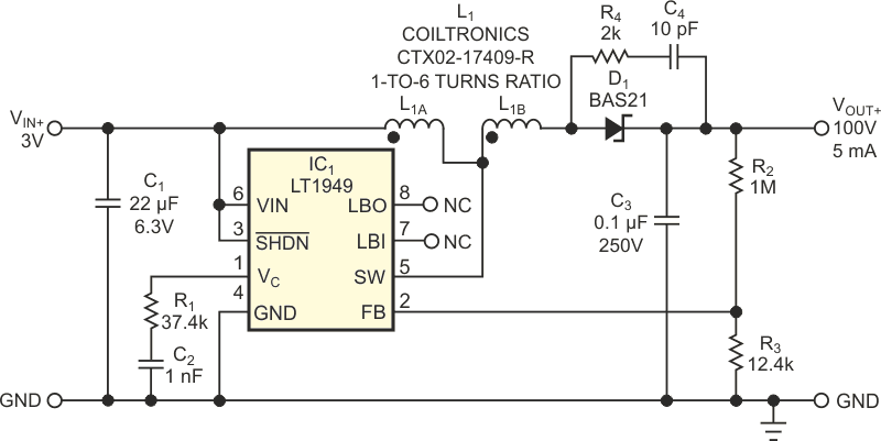
When you face the task of generating a regulated voltage that's higher than the available power-supply voltage, you may consider a boost regulator. Although a boost converter can in theory generate almost any voltage that's higher than its input, practical considerations limit the output to approximately eight times its applied voltage. To generate an even higher voltage, consider using a tapped-inductor boost topology. Figure 1 shows an implementation of a converter that boosts a 3 V input to 100 V dc. The connections to the regulator chip are similar to those of a traditional boost converter, but, to achieve the high boost ratio, this design uses L1, a 1-to-6-turns-ratio, tapped inductor.
 |
|
| Figure 1. | Using a tapped inductor extends a boost-topology switching regulator’s practical output-voltage range. |
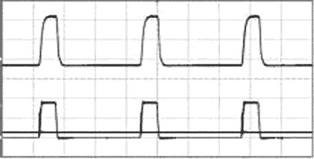
The waveforms in Figure 2 show the input voltage, the voltage at power-switch IC1’s output, Pin 5, and rectifier diode D1’s anode voltage. As in any boost circuit, inductor L1’s core stores energy when IC1’s internal output switch conducts. When the switch turns off, the voltage across its terminals and L1A goes higher than the input voltage. Due to inductive coupling and the larger number of turns that make up L1B, the voltage at rectifier diode D1’s anode and hence the output voltage goes much higher. Resistors R2 and R3 form a feedback-voltage divider that closes the regulation loop. The R4-C4 network forms a snubber circuit that suppresses the impact of diode D1’s small parasitic capacitance. Without the network, power switch IC1 “sees” a capacitance that's 36 times larger due to the multiplicative effect of the tapped inductor's turns ratio.
 |
|
| Figure 2. | For a 3 V-dc input (lower trace, horizontal line), the voltage at regulator IC1’s SW pin reaches a peak of approximately 18 V (lower trace, pulsed waveform). The 1-to-6 step-up turns ratio of inductor L1 further increases the peak output voltage to 160 V (upper trace) to produce 100 V dc. The upper trace’s lower limit goes to –6×VIN (–18 V) due to the tapped inductor. |
Measuring only 5.6×6×3.4 mm, Coiltronics’ CTX02-17409 tapped inductor, L1, and Linear Technology’s LT1949 monolithic regulator, IC1, available in an eight-lead MSOP package, present small pc-board footprints. When you implement the circuit on a single-layer pc board, the entire circuit occupies less than 1.9 cm2 of board space. For best results, review the board-layout suggestions in the device's data sheet and use multilayer-ceramic capacitors for C1 and C3.