New operational amplifiers optimized for high-performance audio and ultrasound applications combine extremely low total harmonic distortion plus noise (THD+N), –130 dB, with large output voltages on heavy, 600-Ω loads. One would think this might be the universal building block.
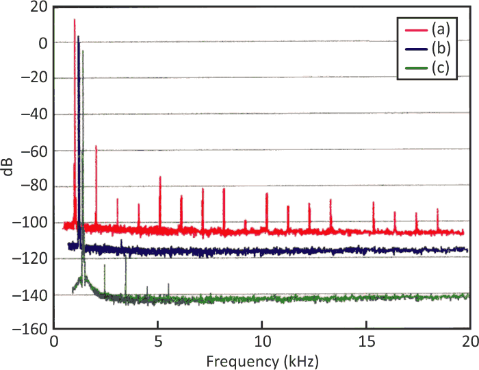
In real life, it’s a bit more complex. For instance, op-amp input capacitance has a nonlinear behavior that’s a function of the input voltage. The associated input current will create a nonlinear voltage drop on the source impedance [1]. Take the distortion spectrum of an LME49710-based unity buffer (Fig. 1, trace a). The signal source is a 5-V rms sine-wave generator with a 1-MΩ source impedance.
 |
|
| Figure 1. | These curves for an LME49710-based standalone unity follower show distortion when fed by a 5-V rms signal source with a 1-MΩ source impedance (a), as well as for the circuit of Fig. 2 fed from the same source (b) and the source generator residual (c). Each subsequent spectrum is shifted +200 Hz and –10 dB for clarity. The higher noise floor for traces (a) and (b) is caused by the thermal noise of the 1-MΩ source resistor. |
Various techniques can reduce these errors, including inverted operating mode, dc biasing, small ac signal swing, proper selection of the op amp, and input impedance compensation [1]. Matching the total impedances seen by the inverting and non-inverting inputs of the op amp provides equal distortion on both inputs, resulting in distortion compensation.
Some signal-processing applications, however, require a front end whose behavior doesn’t depend on source impedance. Examples include data-acquisition systems like oscilloscopes, digitizers, and others that can be connected to the source with high (greater than 50-kΩ) or unknown source impedances.
Another traditional solution to eliminating source impedance-related error involves reducing the input capacitance by bootstrapping the pins of the input device [2], substrate [3], and/or supply rails [4]. Based on its sensed node, bootstrapping can decrease input capacitance, making the op amp faster and shifting the dominant pole to higher frequencies, or it can allow high-voltage applications.
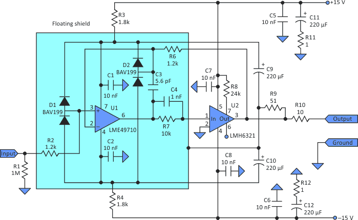
The circuit in Figure 2 achieves high input impedance and negligible source impedance- related error by bootstrapping op-amp U1’s supply rails with the extra follower, U2, and two RC networks (R3-C9, R4-C10). The distortion spectrum of this circuit with a 1-MΩ source (signal generator connected in series with R1) and 50-Ω load is much improved (Fig. 1, trace b). The third harmonic is caused by the generator residual (Fig. 1, trace c). Components C1, C2, and R9 ensure stability in the bootstrap loop.
 |
|
| Figure 2. | Using a circuit that includes a composite unity buffer with supply bootstrapping improves the distortion performance of the device significantly. |
In addition, the composite buffer in Figure 2 completely eliminates power-dissipation-related errors in the op-amp input [1]. Capacitors C9 and C10 can be replaced by adjustable shunt regulators and R3 and R4 by current sources or followers. Subsequently, the circuit will exhibit large input impedance on dc as well.
 |
|
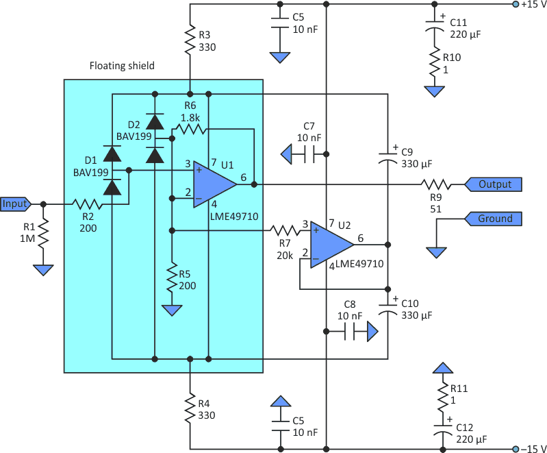
| Figure 3. | With some changes in components, the supply bootstrapping principle can also be used with an amplifier with gain (U2). |
Figure 3 shows how the circuit can be adapted to use an amplifier with gain. Follower U2 provides the current required by bootstrapping circuit R3-R4-C9-C10. The input capacitance of U2 and R7 form a phase lag circuit within the bootstrap loop.
References
- W. Jung, “Op-Amp Audio,” Electronic Design, Sep.-Dec., 1998.
- FET Circuit Applications, National Semiconductor, Application Note 32, Feb. 1970.
- W. Jung, “Bootstrapped IC Substrate Lowers Distortion in JFET Op Amps,” Analog Devices, Application Note 232, July 1992.
- A.M. Sandman, “Reducing Amplifier Distortion,” Wireless World, Vol. 80, No. 1466, pp. 367-371, Oct. 1974.