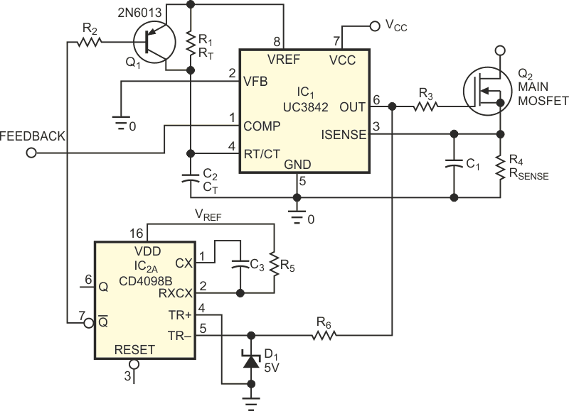
Resonant power supplies are popular because of high efficiency, low noise, and compactness. You can implement a resonant buck or boost converter using a single switch. The regulation of the output in such a converter derives from using a constant on or off time and a variable frequency. The UC1864 controller IC meets all the requirements for a single-switch quasiresonant converter. But you also can achieve this performance with the inexpensive and popular UC3842 current-mode controller in conjunction with a one-shot multivibrator. This circuit gives the desired current-mode operation along with constant off-time, variable-frequency operation. Figure 1 shows the controller circuit, configured as a resonant flyback converter for high-voltage generation. For the implementation of this function, the current-mode controller should have 100% duty cycle; thus, you can use the UC3842 or UC3843. This circuit uses the UC3843. The operation of the circuit is as follows.
 |
|
| Figure 1. | This resonant flyback configuration uses only a controller IC and a one-shot multivibrator. |
The output of IC1, the UC3842, is in a high state until the internal current-sense comparator goes high, and then the output of the IC switches low. As the output voltage goes low, IC2, the negative-edge-triggered one-shot CD4098B, triggers, and it generates a pulse. The pulse duration is a function of the values of R5 and C3, and this time interval is the constant off-time of the UC3842. The /Q output of the one-shot sinks the base current of transistor Q1 during this period, and so the transistor conducts. This action adds a 5 V pulse to the ramp at the RT/CT pin (Pin 4). This voltage remains at 5 V until the pulse ends and /Q goes high. As it goes high, Q1 turns off, but the voltage across CT is 5 V, which is higher than the upper threshold of the RT/CT pin, so the internal circuitry pulls the pin's voltage to zero, and a fresh ramp and a fresh cycle start.
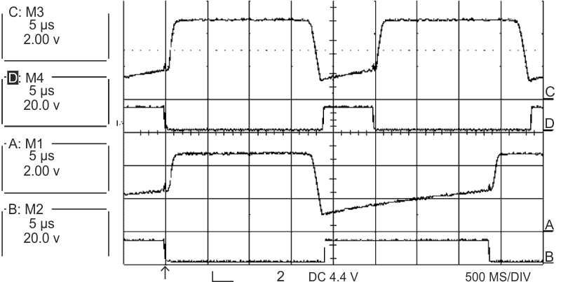 |
|
| Figure 2. | These waveforms typify operation at low (traces C and D) and high (traces A and B) duty cycles. |
You must select RT and CT in such a way that the output voltage goes low before the ramp voltage reaches its upper-threshold level. If not, a glitch can occur in the output, arising from the time constant consisting of the output resistance of Q2 and CT. Figure 2 shows the voltage waveforms at low and high duty cycles. Traces D and C show the output and RT/CT-pin voltages, respectively, at a low duty cycle and, hence, high frequency. Traces B and A show the same voltages, but at a higher duty cycle (low frequency). You can see that the off-time is fixed in both conditions, and only the frequency changes to achieve the desired duty cycle. The voltage at the RT/CT pin gives a clear view of how the circuit modifies the ramp. This control circuit generates a 2-kV, 5-mA dc power supply using a resonant flyback scheme, and it performs well.