Maybe the most common applications for very-low-value resistors (i.e., milliohms (mΩ) and below) are current-controlling circuits, where their low value reduces power losses. For these applications, a tolerance of about 10%-20% is quite sufficient. But even at these tolerances, accurate measurement of very low resistance values can be rather difficult, especially when a large current is involved.
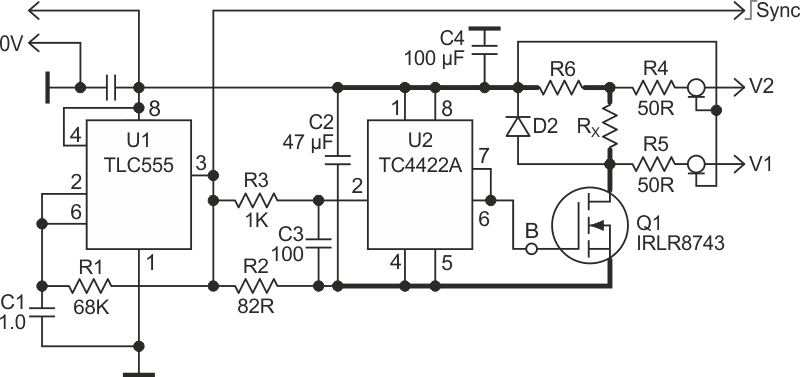
The circuit shown in Figure 1 provides a solution to the problem by applying a low duty cycle pulse to the unknown resistor and a reference resistor of a known value. A ratiometric technique is used to compare the response of the two components and determine the value of the resistor under test.
 |
|
| Figure 1. | The circuit shown enables accurate measurement of very low resistance values by applying a low duty cycle pulse to the unknown resistor and a reference resistor of a known value. |
The measurements needed to calculate accurate resistance values can be obtained from the outputs V1 & V2 using an ordinary oscilloscope or, instead, a pulse peak voltmeter, which can provide higher precision.
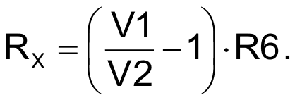
The circuit uses the venerable 555 timer, running in an astable mode to produce pulses that are used to charge and discharge a low-inductance capacitor C2. During the discharge cycle, the current is passed through a precision standard resistor (R6) and the resistance under measurement (RX). The value of the resistance can be calculated from the ratio of the corresponding voltages:
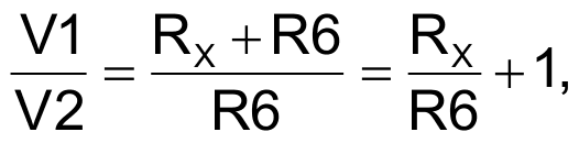
where V1 and V2 are peak values.
Hence, the unknown value:
The bandwidth of the scope/voltmeter should be large enough to catch the short pulses produced by the circuit. Some scopes would not ensure a sufficient brightness because of the very large ratio of the half-period of the 555 oscillator and the duration of the pulse.
The circuit can be used also to drive other low-resistance loads that require large-amplitude, low-duration current pulses, such as a semiconductor laser.
Test circuit details
The pulse Sync (U1, pin 3) facilitates the earlier synchronization of the scope; the delay between the Sync and the output pulse may allow the scope to catch the front of the pulse, since some scopes may have no delay line in their Y channel, making very steep fronts un-displayable. This delay is determined by the time constant R3•C3. The value of C3 may be in the range 20 – 500 pF (or even more), depending on the time base used and the scope itself.
The MOSFET driver U2 (TC4422A) is used to ensure high gate charging current for Q1 and fast switch-on time, which are essential for accurate measurements.
The MOSFET (Q1) has very low RDSOn (sub-3 Ω), to insure a clean, high-amplitude pulse. Fast diode D2 limits an overvoltage of Q1. Note: high currents occurring in this part of the circuit require special attention to both component selection and PCB layout. See the Component Selection Notes and Design Notes sections below for details.
The circuit’s short and powerful current pulse also creates a broad-spectrum response in the frequency domain. So careful attention must be paid to minimize parasitic inductive and capacitive loads or the circuit will display high levels of reactance and resulting oscillations in various parts of the layout. The practical details you’ll need to know about how to minimize these unwanted parasitics are documented in the Design Notes section of this article.
Component selection notes
SMD components are highly recommended for the circuit. Some capacitors, even with a film-based structure, can experience piezoelectric movement in their dielectric layers when subjected to sharp, high current pulses, similar to those C2 is exposed to. Sometimes you can even hear quite audible ‘ticks’ from such capacitors, which means high level of losses due to the piezoelectric effect. In this case, the component with the lower level of ‘ticks’ can be regarded as a better one.
A 0.005 Ω (5 mΩ), 1% tolerance LOB-3 precision resistor from TT Electronics was used as the standard resistance (R6).
Due to the ratiometric measurement technique employed by the circuit, the tolerances of most components are not very critical, but special attention should be paid to their stability and construction style. For instance, the value of the capacitor C2 is not critical, but it should be large enough to provide a sufficiently long current pulse, easily noticeable by your scope or voltmeter.
This capacitor should use a construction technique such as stacked-foil film or ceramic with low internal resistance/inductance. You should avoid many types of capacitors, especially ceramic, if their capacitance depends on the voltage applied. If necessary, several capacitors may be connected in parallel to produce the desired value.
For the MOSFET, good examples with very low RDSon are the CSD16321Q5 from TI or IRLx8743 from IR. However, such devices often have a comparatively low drain-to-source and gate-to-source breakdown voltage (only 8 V for CSD16321Q5) – a potential weak point that should be taken into account for any modifications you make.
Another potential restriction is the maximum drain current of the MOSFET. Both of these parameters affect the test circuit’s lower measurements limit.
To reduce the level of parasitic oscillations, the resistor R6 and capacitor C4 should have very low inductances – both the components themselves, and the PCB traces they are connected to.
Design notes
The PCB traces around R6 and C4 must be kept short and laid out in order to minimize the parasitic reactances, which can lead to local resonances stimulated by the current pulses. If the circuit layout does not comply with this requirement, the absolute maximum voltage rating of MOSFET Q1 can be easily exceeded. For example, for a capacitive load of 6 nF (gate capacitance) the output rise/fall times of the driver TC4422A can be less than 25 ns; this fact, together with a large current (~100 A) through the inductances can produce voltages that would damage nearly any MOSFET.
Refer to the schematic to see the traces highlighted in bold – these traces must be wide enough to carry the high currents and be kept as short as possible to minimize parasitic inductance. This is especially critical for the trace connecting the gate to the driver (U2, pin 6 to base of Q1), which should be kept to less than one inch. A ferrite bead on this trace (B) can help suppress the unwanted oscillations.
For the same reason, the connections of the both resistors RX and R6 should be as close to the same length as possible. They should also be as short as possible to minimize inductances and voltage drops.
All external connections to the circuit should be designed using basic high-frequency practices. For example, using 50-Ω coax cables with good impedance matching on both ends is a must.