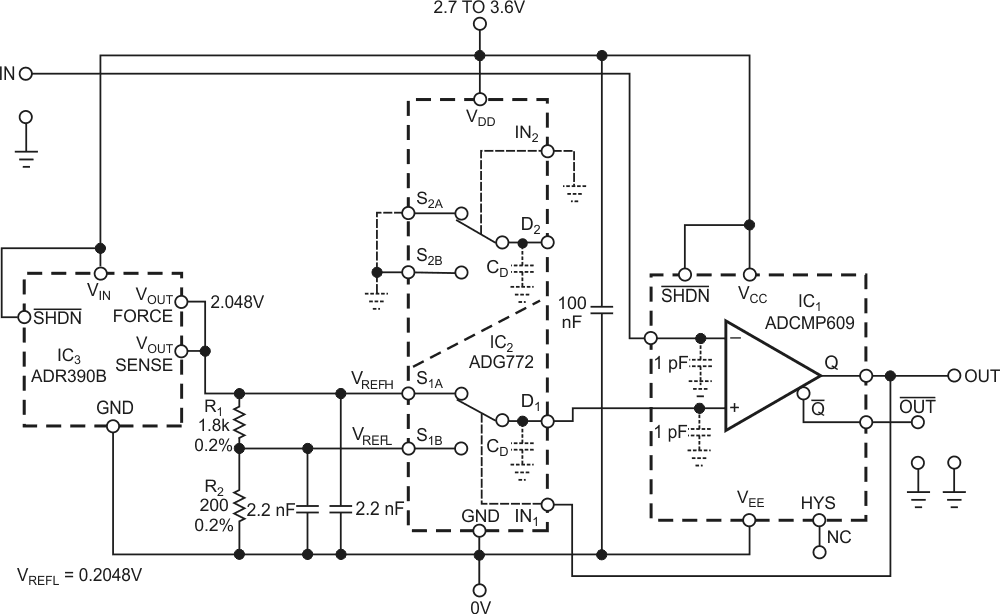
In advanced IC comparators, programmable hysteresis eliminates 0V-centered differential-input-voltage noise and improves the comparator’s response if its differential-input voltage is low or varies slowly over time. For example, the ADCMP609 comparator from Analog Devices lets you program its hysteresis from 0 to 160 mV with a single resistor that connects between the HYS (hysteresis) pin and ground. That voltage range may be too narrow for some applications, however. The circuit in Figure 1 lets you widen the hysteresis by using two reference voltages applied to the noninverting input. The circuit uses IC3, an Analog Devices ADR390B, to generate a high reference voltage, VREFH, of 2.048 V. Resistor divider R1/R2 produces a low reference voltage, VREFL, of 0.2048 V, or a difference of 1.8432 V. Thus, the hysteresis equals the high reference voltage minus the low reference voltage. IC2, an Analog Devices ADG772 dual-SPDT (single-pole/double-throw) switch, routes the voltages to the comparator’s noninverting input.
 |
|
| Figure 1. | An analog switch changes the comparator’s reference voltage, thus increasing hysteresis. |
Whenever the input voltage at the comparator’s inverting input exceeds the high reference voltage, the output goes to a logic low. That action forces S1B to connect the low reference voltage to the comparator’s noninverting input. The circuit remains in that state until the input voltage drops below the low reference voltage. At that point, the switch connects the high reference voltage back to the comparator. For fast-ramping waveforms at the input, the hysteresis increases because of signal-propagation delays in both IC1 and IC2. The 35-nsec propagation delay in the ADCMP609 occurs at approximately 10 mV of input overdrive, and this overdrive roughly doubles in effect as an addition to the hysteresis voltage, increasing it by approximately 1%.
Because ADCMP60x comparators are rail-to-rail I/O devices, the low reference voltage could be 0 V. In this case, however, the value of 0.2048 V lets the comparator cooperate with other rail-to-rail I/O ICs from the same supply voltage. The outputs of these ICs can swing between 0 V and the power-supply voltage with a margin of millivolts to tens of millivolts, depending on the load. An ADR390B provides the reference voltages. The 2.2 nF decoupling capacitors suppress variations of these voltages during voltage transitions at the Q output. These values are sufficient because the parasitic-charge transfer from the switch’s control input, IN1, to the respective channel’s source electrode is typically 0.5 pC. The short-term variation of the decoupled reference voltages is less than 250 µV.