Low-voltage microcontrollers generally have been powered from a regulated supply, such as 1.8 to .6 V, and have very low current consumption, typically between 1 mA and 5 mA. Achieving an inexpensive, space-saving solution for effective conversion from line voltage as high as 230 V ac down to 3 V/20 mW is not a simple task, especially while meeting additional mandates such as those for electromagnetic compatibility (EMC) and standby power.
The non-isolated supply converter shown requires no inductor or switched-mode power (SMP) converter. It uses the “capacitive-dropper principle” enhanced with a new and specific connection of the Q-pump (a capacitor-based charge pump), which converts the power in the opposite direction, from minus node to plus node.
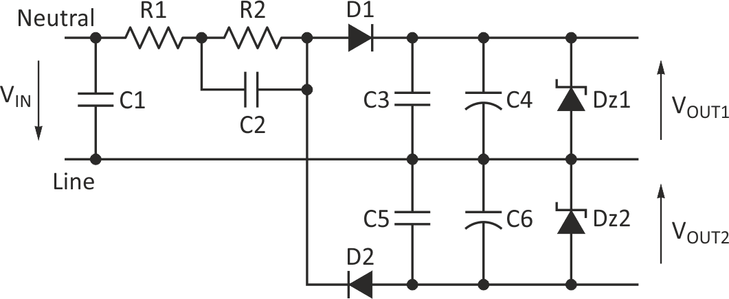
In the well-known design of a capacitive power supply, capacitor C2 accommodates the ac mains voltage to a voltage level suitable for the application, while R1 and R2 are connected to limit inrush currents due to the capacitors (Fig. 1). The voltage is then rectified by diodes D1 and D2 and regulated using Zener diodes Dz1 and Dz2 along with output capacitors C4 and C6. The amount of output current depends on the impedance of capacitors at 230 V/50 Hz or 110 V/60 Hz.
 |
|
| Figure 1. | The basic capacitive converter uses a diode rectification, Zener diodes, and capacitors but has no regulation. |
Capacitor C2 must be the X2 type to satisfy EN 60384-14. Resistor R2 builds a discharge path for C2, still meeting IEC61010-1 or UL1950 safety requirements. The output current of the converter is determined according to:
IOUT_EFF = ULINE × 2π × fLINE × C2,
where ULINE and fLINE are the line voltage and frequency, respectively.
Recently, Murata introduced a very small and interesting monolithic ceramic chip capacitor, the SMD-X2. For a 230-V ac line, the output current with this capacitor is:
IOUT_EFF = 230 × 2π × 50 × 56 × 10 – 9 = 4.0 mA,
for 110 V ac, it is:
IOUT_EFF = 2.3 mA.
While this might be enough current for many very low-power microcontroller applications, it wouldn’t be sufficient for many of them. In the modified capacitive converter, diodes D1 and D2 have been replaced with a bridge comprising D1, D2, D3, and D6, which pumps current into capacitor C1 in every half-period of line voltage (Fig. 2). Varistor U2 and suppressor U1 are added for immunity against 2-kV surge and the burst testing procedure of IEC61000-4-5.
 |
|
| Figure 2. | The modified capacitive converter with bridge rectifier adds additional regulation and protection. |
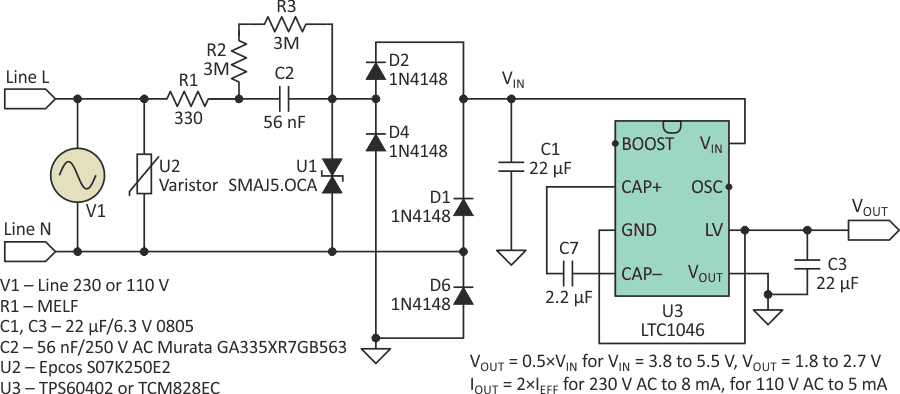
I used the LTC1046, which has a model in SW-LTspice, for the simulation of the circuits model of the Q-pump. However, it is too expensive for many situations, so you can use the TPS60402 or TMC828EC, which have the same functionality but are cheaper.
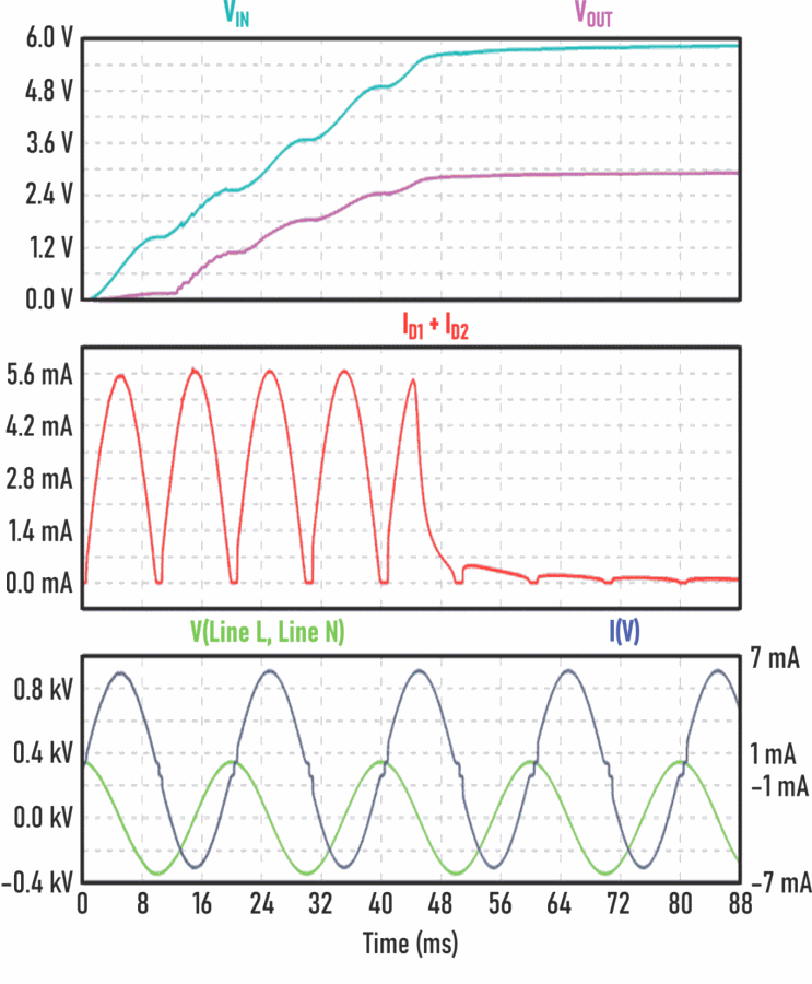
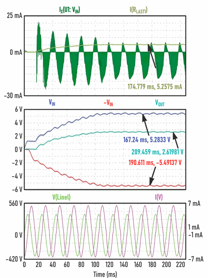
Therefore, there is only a very short time when the charge from C1 has to supply the rest of the circuit. The circuit has been simulated using LT-Spice version 4.19, as well as built and tested (Fig. 3).
 |
|
 |
|
| Figure 3. | C1 has to supply the rest of the circuit of Figure 2 for very short periods. |
U3 is the capacitor-based charge pump, a very cheap, small (SOT23-6), and very efficient IC for small currents. In the step-down charge pump connection, it produces output voltage VOUT = 0.5 × VIN and corresponding output current IOUT = 2 × IIN. With the same 56-nF X2 capacitor for C2, we get IOUT_EFF = 8.0 mA for the 230-V ac line and IOUT_EFF = 4.6 mA for the 110-V ac line. This should be sufficient for most modern microcontrollers with a supply voltage range between 1.8 V and 2.7 V.
The “ground” of the converter is not connected with any side of ac-supply lines. Instead, it alternates between both line and neutral. As such, it could be unsuitable for many applications. To overcome this, the modified schematic uses the same arrangement of two-way rectification as the basic design in Figure 1, bringing a fixed connection of the ground supply node to one of the line wires (Fig. 4).
 |
|
| Figure 4. | The modified capacitive converter without bridge rectifier brings a fixed ground connection. |
The value of capacitor C5 for the negative rectification path is two to three times larger than the value of capacitor C1 for the positive path. As a result, the voltage on the positive path grows more quickly than it does on the negative path. The Q-pump-IC is designed to convert a positive supply into a negative one, using a bridge of four controlled-FET switches and a working capacitor. The opposite conversion of energy can be produced from the negative path of the supply to the positive path, due to the use of these FETs for switching.
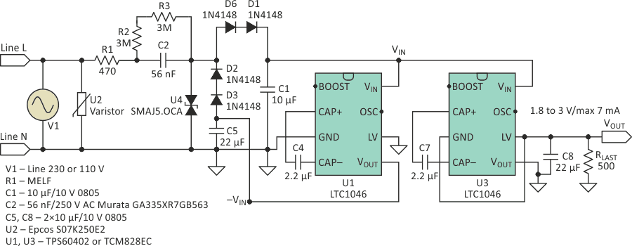
This results in the same properties in this rectification circuit as with bidirectional rectification using a diode bridge. Figure 5 shows the simulated results and the change of current polarity of charge pump U1’s VIN pin.
 |
|
| Figure 5. | The startup and normal operation of the circuit at 230 V ac shows the change of current polarity on the VIN of charge pump U1 with a cycling period of 5 ms and 15 ms. |
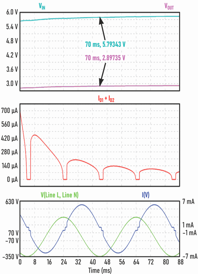
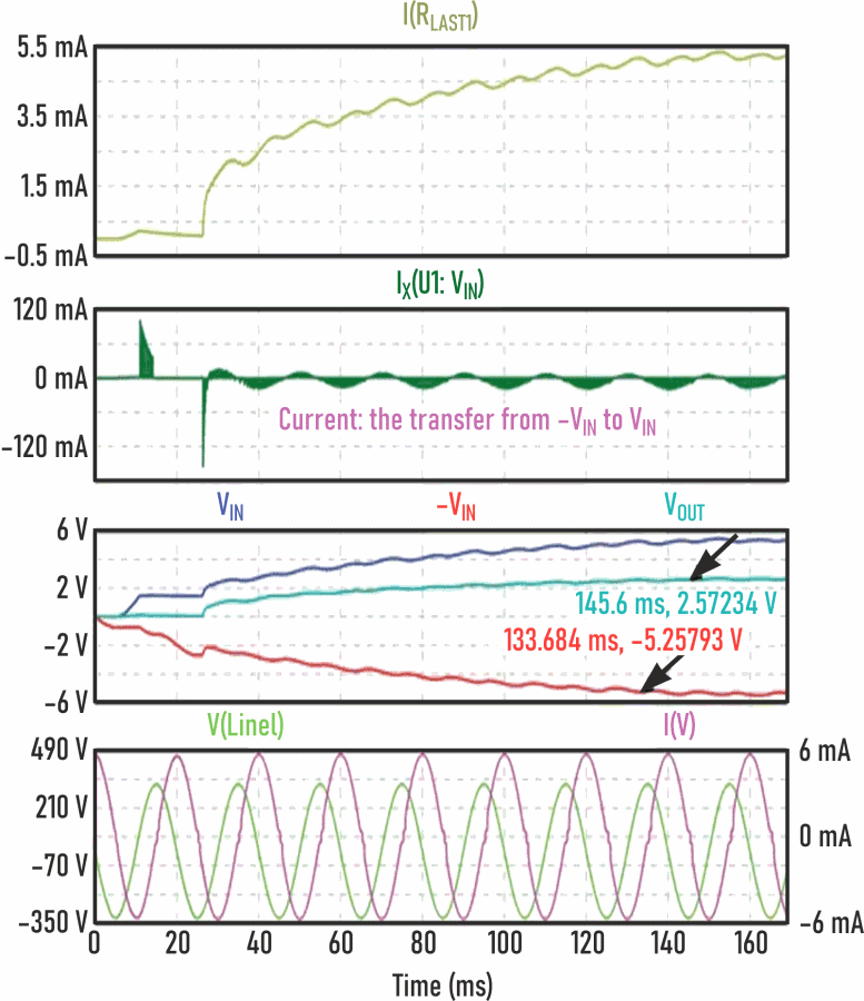
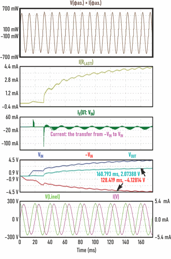
The circuit of Figure 5 has been simulated and tested at the worst-case line voltage of 230 V ac ±20% (Fig. 6).
|
|||||
| Figure 6. | The waveforms of critical circuit points at startup and during normal operation of the circuit at a low line-voltage of 184 V ac (a) and a high line-voltage of 260 V ac (b) show smooth power-on transition and subsequent regulation. |
||||
All results meet the requirements for most modern MCUs with respect to 2013 ErP Standby Power Regulation (see Table 1).
| Table 1. | Key operational parameters at 184-, 230-, and 260-V AC line voltages |
||||||||||||||||||||||||
|
|||||||||||||||||||||||||
There was a very small ripple in VOUT (<60 mV) for capacitor C5, 100 µF/10 V (Taiyo Yuden LMK325BJ107MM), and C1, 22 µF/10 V (Murata GRM219B31A226MEA 0805). Also:
- The less complicated circuit of Figure 2 can be used for applications that don’t need a fixed connection to the power line (line or neutral).
- Two 56-nF, X2-type capacitors should be used in parallel for applications with a line voltage of 110 V ac or universal input from 85 to 260 V ac.
- There is a minimum 12- by 12- by 8-mm space required for this design on a two-layer printed-circuit board.
- To stabilize the output voltage over line voltage 230 V ac ±20%, use consecutive low-dropout regulators such as the TLV70025.