Vassilis Papanikolaou
This is a new design of a tutorial board based on the popular PIC16F84A microcontroller. It features eight single leds, a 7-segment display, an LCD display and five push buttons. It is an ideal solution for the beginner to take his/her first programming steps in the world of microcontrollers. Having an in-circuit-programming (ICP) header, it can be easily reprogrammed without unplugging the microcontroller each time, provided that the programmer also supports this feature (like OziPic’er).
 Click to enlarge |
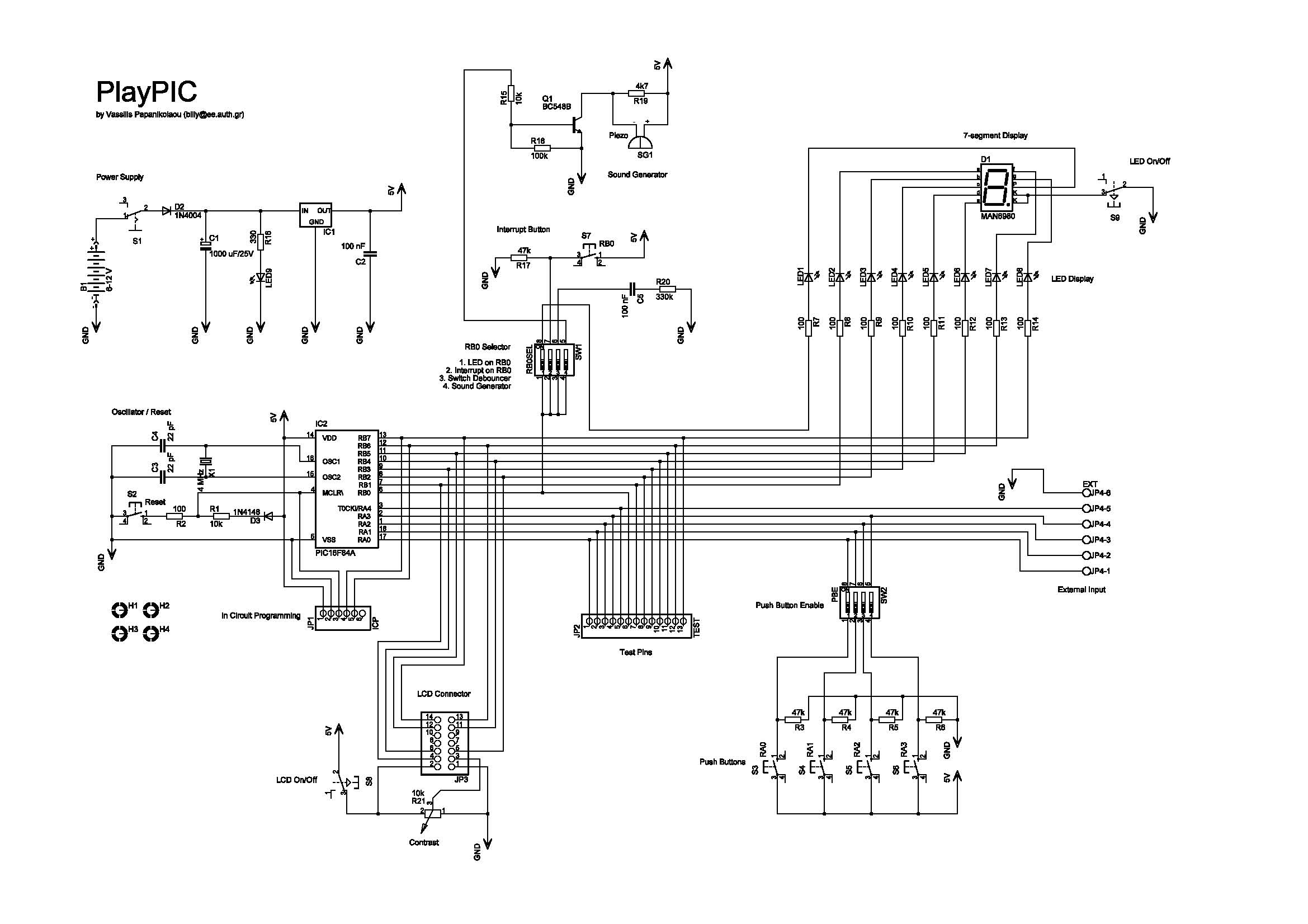
| PlayPIC Schematic |
Connections
|
PIC16F84A |
Feature |
|
RA0 |
JP2 – S3 – JP4 |
|
RA1 |
JP2 – S4 – JP4 |
|
RA2 |
JP2 – S5 – JP4 |
|
RA3 |
JP2 – S6 – JP4 |
|
RA4 |
JP2 – JP4 |
|
RB0 |
JP2 – LED1 – 7 Seg (dp) – S7 Debounce – Buzzer |
|
RB1 |
JP2 – LED2 – 7 Seg (a) – LCD RS |
|
RB2 |
JP2 – LED3 – 7 Seg (b) – LCD R/W |
|
RB3 |
JP2 – LED4 – 7 Seg (c) – LCD E |
|
RB4 |
JP2 – LED5 – 7 Seg (d) – LCD DB4 |
|
RB5 |
JP2 – LED6 – 7 Seg (e) – LCD DB5 |
|
RB6 |
JP2 – LED7 – 7 Seg (f) – LCD DB6 |
|
RB7 |
JP2 – LED8 – 7 Seg (g) – LCD DB7 |
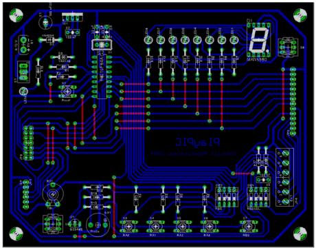 |
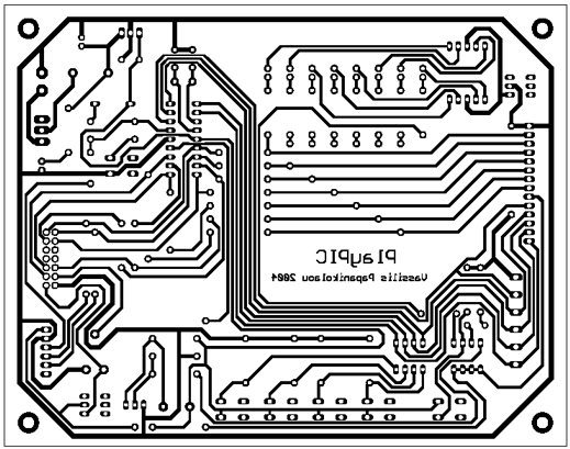
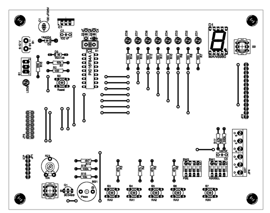
| PlayPIC PCB |
Feature Description
- S1 switches the board on and off. When on, the indicator led LED9 is lit.
- S2 resets the microcontroller.
- S8 switches the LCD display on and off.
- S9 switches the eight individual leds AND the 7-segment display on and off.
- Push buttons S3 to S6 correspond to RA0-RA3 inputs. They are enabled or disabled by the SW2 dip switch.
- The SW1 dip switch enables or disables the following features :
- Connects RB0 (used as output) to LED1.
- Connects RB0 (used as interrupt input) to S7.
- Enables the debouncing circuit for interrupt switch S7.
- Connects RB0 (used as output) to the buzzer.
This dip switch must be either 1000 or 0100 or 0110 or 0001.
- The 7-segment display is always connected to the individual leds. Its seven segments correspond to LED2 to LED8 (RB1 to RB7) and the decimal dot to LED1 (RB0). This correspondence enables the 7-segment display to work together with the interrupt switch S7, which is connected to RB0.
- JP4 is an 6-screw external input connector for RA0-RA4. When used, the corresponding input switches S3-S6 must be turned off by SW2. Last screw is ground.
- JP2 is a 14 pin test terminal. A voltmeter or logic analyzer can be connected any time to monitor the signal traffic in the circuit. Last pin is ground.
- JP1 is the ICP header. When in-circuit-programming is performed, the board must be OFF (by S1), as well as the LCD (by S8) and leds (by S9).
- JP3 is a 14-pin connector for the LCD module. Contrast can be adjusted by trimmer R21.
- - The board can be powered either by a 9V battery or a 6-12 V power supply.
PDF versions of the schematic and PCB are included. The board has been sucessfully build and it is depicted on the following
Photos :
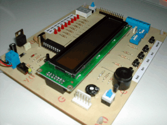 |
|
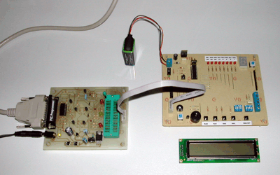
The right photo shows the in-circuit-programming procedure with the help of an appropriate programmer (like OziPic'er) which features an ICP header. In order for the procedure to work correctly, the LCD module has to be disconnected from its socket during programming.
Any futher ideas, comments and corrections are mostly welcome to billy@ee.auth.gr
 Click to enlarge |