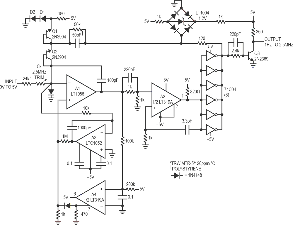
Figure 1’s circuit is not as fast as some other circuits, but its 2.5 MHz output settles from a full-scale input step in only 3 μs. This makes the circuit a good candidate for FM applications or any area where fast response to input movement is required. Linearity is 0.05% with a 50 ppm/°C gain tempco. A chopper-stabilized correction network holds zero-point error to 0.025 Hz/°C. This circuit, a high speed charge-dispensing type also uses charge feedback. The charge feedback scheme used is a highly modified, high speed variant of the approach originally described by R. A. Pease (Reference 1). A servo amplifier is not used, permitting fast response to input steps. Instead, the charge is fed back directly to the oscillator, which can respond immediately. Although this approach permits fast response, it also requires attention to parasitics to achieve high linearity and low drift.
 |
|
| Figure 1. | 1 Hz to 2.5 MHz fast response V-F. |
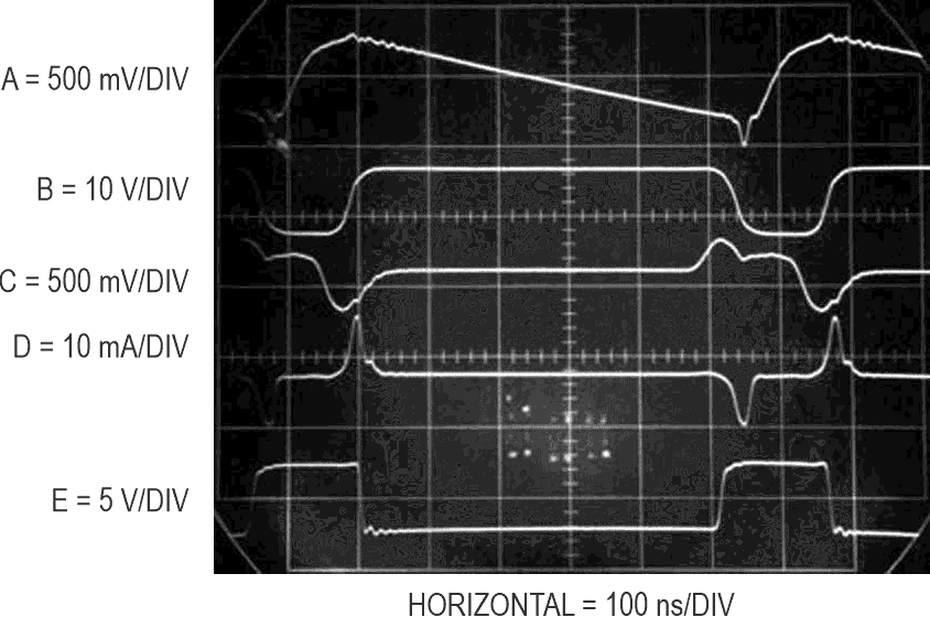
When an input voltage is applied, A1 integrates in a negative direction (Trace A, Figure 2). When its output crosses zero, A2’s output switches, causing the paralleled inverters to go low (Trace B). The feedforward network in A2’s negative input aids response. This causes the LT1004 diode bridge to bound at –2.4 V (–VZ LT1004) + (–2VFWD). Local positive feedback at A2’s positive input (Trace C) reinforces this action. During this interval, charge is pulled (Trace D) from A1’s summing junction via the 50 pF-50k combination, forcing A1’s output to move quickly positive. This causes the A2 inverter combination to switch positive (Trace B), bounding the LT1004 diode bridge at 2.4 V. Now the 50 pF capacitor receives charge, while A1 again integrates negative, and the entire cycle repeats. The frequency of this action is a linear function of the input voltage.
 |
|
| Figure 2. | Fast response V-F waveforms. |
D1 and D2 compensate the diodes in the bridge. Diode-connected Q1 compensates steering diode Q2. (The diode-connected transistors provide lower leakage from the summing junction than conventional diodes.) A3, a chopper-stabilized op amp, offset stabilizes A1, eliminating the necessity for zero trimming.
A4 guards against circuit latch-up, which can occur due to the AC-coupled feedback loop. If the circuit latches, A1’s output goes to the negative rail and stays there. This causes A4’s output (A4 is used in emitter-follower output mode) to go high. A1’s output now heads positive, initiating normal circuit behavior. The diode at A1’s negative input ensures that the start-up loop will dominate over any input condition.
The 50k resistor across the 50 pF charge-dispensing capacitor improves linearity by permitting complete discharge on each cycle, despite junction tailing effects in Q2. The input resistor specified has a temperature coefficient opposite that of the capacitor’s enhancing circuit gain tempco.
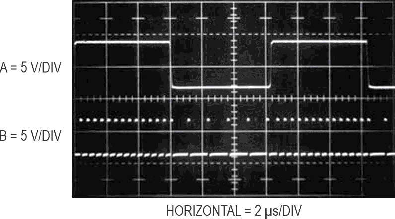
Figure 3 shows circuit step response. Trace A is the input, while Trace B is the output. Frequency shift is quick and clean, with no evidence of poor dynamics or time constants.
 |
|
| Figure 3. | Step response of 2.5 MHz V-F. |
To trim the circuit, apply 5.000 V and adjust the 5k potentiometer for a 2.500 MHz output. A3’s low offset eliminates the requirement for a zero trim. The circuit maintains 0.05% linearity with 50 ppm/°C drift from 1 Hz to 2.5 MHz. The TTL-compatible output is available at Q3’s collector (Trace E).
Reference
- Pease R. A., “A New Ultra-Linear Voltage-to-Frequency Converter,” 1973 NEREM Record, Vol. I, page 167.