No currently available V-F converter will accept bipolar (AC) inputs. This feature is desirable in power line monitoring and other applications. Figure 1’s V-F converter accepts ±10 V inputs, producing a 0 kHz to 10 kHz output. Linearity is 0.04%, and temperature coefficient measures about 50 ppm/°C.
 |
|
| Figure 1. | Bipolar (AC) input V-to-F converter. |
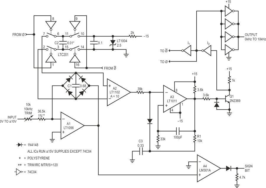
To understand circuit operation, assume a bipolar square wave (trace A, Figure 2) is applied to the input. During the input’s positive phase, A1’s output (trace B) swings negative, driving current through C1 via the full wave diode bridge. A1’s current causes C1 to ramp linearly. Instrumentation amplifier A2, operating at a gain of 10, looks differentially across C1. A2’s output (trace C) biases comparator A3’s negative input. When A2’s output crosses zero, A3 fires (trace D). AC positive feedback to A3’s positive input (trace E) “hangs up” A3’s output for about 20 ps. The Q1 level shifter drives ground referred inverters I1 and I2 to deliver biphase drive (traces G and H) to the LTC201 switch. The LTC201, set up as a charge pump, places C2 across C1 each time the inverters switch, resetting C1 to a lower voltage. The LT1004 reference, along with C2’s value, determines how much charge is removed from C1 each time the charge pump cycles. Thus, each time A2’s output tries to cross zero, C2 is switched across C1, resetting it to a small negative voltage and forcing A1 to begin recharging it. The frequency of this oscillatory behavior is directly proportional to the input derived current into A1. During the time C1 is ramping toward zero the LTC201 switches C2 across the LT1004, preparing it for the next discharge cycle. The action is the same for negative input excursions (see Figure 2), except that A1’s output phasing is reversed. A2, looking differentially across A1’s diode bridge, sees the same signal as for positive inputs and circuit action is identical. A4, detecting A1’s output polarity, provides a sign bit output (trace F).
 |
|
| Figure 2. | Bipolar (AC) input V-to-F converter. |
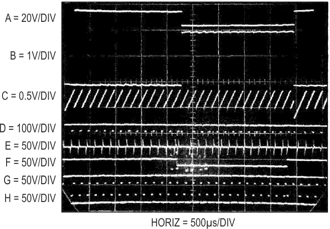
Figure 3, an amplitude expanded version of A1 and A2’s outputs, shows detail. Trace A is the input, while trace В and trace С are A1 and A2’s outputs, respectively. Complementary bias points and ramping action are clearly visible in A1’s output, while A2 responds identically for both input phases. A1’s output bias points are established by the two conducting bridge diodes. When the input switches polarity, A1 responds immediately and oscillation frequency settles within 1 to 2 cycles of final value.
 |
|
| Figure 3. | Detail of integrator and differential amplifier outputs. |
Start-up or overdrive conditions could cause this loop to latch. A start-up mechanism, adapted from oscilloscope trigger circuitry, precludes latch-up. If C1 charges past the point where C2 can reset it, loop closure ceases. A2’s output saturates positive, causing A3 to go negative. A3’s prolonged negative state, detected by the R1-C3 filter, pulls its negative input toward –15 V. When A3’s negative input crosses zero, its output changes state and charges R1-C3 positively. A3’s input rises above zero, causing output reversal and free-running oscillation commences. As in normal mode, the 100pF-33k RC aids transitions. A3’s oscillations are transmitted to the LTC201 based charge pump via A1 and the inverters. C2 pumps charge out of C1, driving the voltage across it toward zero. A2 comes out of positive saturation and heads negative, eliminating positive bias at A3’s input. A3’s free-running oscillation stops, and normal loop action begins.
To calibrate this circuit apply either a –10 V or a +10 V input and set the 10 kΩ trimmer for exactly 10 kHz output. The low offsets of A1 and A2 permit operation down to a few hertz with no zero trim required.